Karthik Rao, Nitin Goel, Prashant Bhargava - Freescale Semiconductor India Pvt. Ltd.
March 11, 2013
Synchronous interfaces involve a single clock domain and are relatively easy to design. However, at times, it is advantageous and necessary to have an asynchronous interface between peripherals for increased robustness. Asynchronous designs include multiple clock domains running at different frequencies and clock phases. Some clock domains may be shut down when not needed which helps in saving power and increasing efficiency. To avail these benefits on a stable synchronous design, converting it into an asynchronous design may be considered.
This article deals with various challenges faced in modifying a synchronous design to an asynchronous one. It aims to provide a brief overview of design and verification aspects to consider while making this transition.
Introduction
As an example, a reference design is considered which is synchronous in nature, i.e. all sequential logic in the design is clocked from a single clock source or its derivatives. The figure below shows a basic synchronous design block. Such design blocks essentially consist of register interface logic, control logic and the intended module specific operation logic (for example a communication protocol).
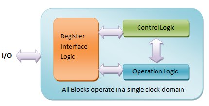
Figure 1: Synchronous Design Block
Since all sub-blocks shown in Fig. 1 are clocked by a single clock source or its derivatives, there is no requirement for synchronization between the sub-block interfaces. However, if the application requires specific part of the logic in the above design block to run on a higher frequency, it will necessitate other sub-blocks in the design to run on the same higher frequency as well. This would lead to overall rise in power consumption and silicon area occupied by the design (since now timing must be met on a higher frequency) along with introduction of tighter constraints on the clock tree and routing for the design block.
Another limitation with a synchronous design block is related with Low Power Mode or Standby Mode in an application, where most functional blocks except critical operations are halted or disabled to minimize power consumption. Shutting down clocks to certain blocks, which are not required for Standby Mode, helps bring down power consumption. But this is not feasible in a synchronous design block since there is only a single clock source and it is required to operate in a low power or standby mode. The ideal behavior would be to shut off clock to register interface and part of control logic and keep the protocol specific logic active. Now, achieving this behavior in a module which is designed from scratch is easy but adding clock domain partitioning in a stable and verified synchronous module throws up many design and verification challenges.
The key to achieving successful partitioning of a synchronous design into an asynchronous one is to identify the correct design portioning and placing appropriate synchronization schemes between the asynchronous clock domains. The importance of selecting the right synchronization scheme is highlighted from the fact that the design has to work for any clock ratio. Either clock could be faster or slower. The synchronization scheme has to handle this.
On a broader level, the design considerations can be broken down to be associated with Data synchronization or Control Logic synchronization. For most design categories, a synchronous design block is considered and suggestions for asynchronous counterparts are explained.
Data Synchronization
Data Queues
The synchronous design might include queuing structures (e.g. FIFO, etc.) for handling data storage. The ‘store’ and ‘fetch’ operation of such a queue runs on the same clock. Depending on design requirements, these operations in the asynchronous design counterpart would need to run on separate clocks in which case, queuing structure needs to be modified to support asynchronous interfaces.
Consider an asynchronous FIFO for example: The general approach of designing an asynchronous FIFO is shown in Figure 1.
Since data ‘read’ and ‘write’ operations on this FIFO work on separate asynchronous clocks, special care must be taken while generating the ‘Full’ and ‘Empty’ flags. An overflow or underflow condition causes the data corruption or data loss. Safe and reliable FIFO designs always avoid both extreme conditions. The usual approach is to compare the read and write pointers for generating the status flags. But in an asynchronous FIFO, either of the pointers needs to be synchronized before comparison. Hence the ‘Full’ and ‘Empty’ conditions would really mean ‘almost full’ and ‘almost empty’ respectively to maintain reliability.
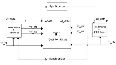
Figure 2: General approach to asynchronous FIFO design
Another factor to consider is the size of the FIFO. In the synchronous FIFO, since reads/writes could operate at same speeds, size was not an issue. But in its asynchronous counterpart, reads/writes both can operate on separate clocks. Hence the optimum size requirement for the target application must be computed.
Sampling Asynchronous Data Inputs
A synchronous design samples internal data signals which lie in the same clock domain as the design itself. However, for its asynchronous counterpart, the design block can sample data that is located in a different or asynchronous clock domain. Hence this data would need to be synchronized before being used.
This poses a unique problem to the design. The time needed for such synchronization depends on the relationship of the clock domains across which the data is being synchronized. It must be ensured that the rate of change of such data does not exceed the time needed for its synchronization; else data loss would occur at the clock boundary. Thus the clock ratio controls or ‘constraints’ the rate of change of input data that is to be synchronized.
For example, consider a “Receiver Block” which receives serial data frames continuously at fixed intervals. This data is stored in the ‘Receive register’ from which the CPU fetches the data for further usage. The receive register is used to latch subsequent received frames. Since the input data is asynchronous to the receiver block, the received data would have to be synchronized before it latches onto the receive register. As explained before, this introduces speed constraints on the data being received given by the following equation.
TDin > Tsync
Where TDin is the minimum time available before current input data frame is replaced by a subsequent one and Tsync is the time taken to synchronize the received frame.
If such constraints are unacceptable, then an asynchronous FIFO-like structure could be thought of to get rid of these constraints. That would be an example of sacrificing area to ease constraints.
Control Logic Synchronization
Clock Ratios
With the introduction of multiple clock domains into the design, there arises a unique issue which never existed in synchronous designs i.e. transferring signals from faster clock domain to a slower one.
In such scenarios, the signal in the source (faster) clock domain can be too small and could be completely missed by the destination (slower) clock domain. Figures 3 and 4 illustrate this problem.

Figure 3: A two Flop synchronizer with higher source frequency
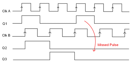
Figure 4: Timing Diagram for the synchronizer block with higher source frequency
One approach to solve this issue is to hold (elongate) the signal in the (source) faster clock domain for at least a single clock period of the destination (slower) domain so that the signal is guaranteed to be sampled and synchronized into the destination clock domain.
If holding the source signal is not feasible, then another approach can be considered, in which the rising (or falling) edge of the control signal is used as a clock input into a D Flip-Flop whose D input is tied to 1. The output of such a flop is synchronized into the destination (slower) domain thus transferring the signal from the faster clock domain successfully into the slower domain as illustrated in Figure 5.
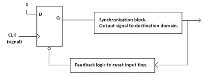
Figure 5: Edge capture circuit
Asynchronous Resets
In case of multiple clock domains, flops work with asynchronous resets. One of the major problems with asynchronous resets is the reset release, also called reset removal.
The resets are asynchronous both at assertion as well at de-assertion of resets. The assertion is not an issue while de-assertion is a concern. If the asynchronous reset is released at or near the active clock edge of a flip-flop, the output of the flip-flop could go meta-stable and thus reset state of the design block could be lost.
Hence every design using an asynchronous reset should include a reset synchronizer circuit. Such a circuit should ensure that even though reset assertion takes place asynchronously, reset de-assertion must always be synchronous to the clock of respective asynchronous clock domains.
Register Reads/Writes
In a synchronous design, register write operation usually takes effect on the next clock while register read operation completes on the same clock (since read logic can be combinational in nature).
In the asynchronous design counterpart, some or all registers may fall under separate asynchronous clock domains in relation to the register interface domain. For such cases, appropriate number of wait states must be added when accessing such registers.
Post Design Stage
While transitioning a design from synchronous domain to asynchronous domain, there are certain considerations in verification which need to be accounted for in order to have a good quality design that can be seamlessly integrated into a SOC.
Verification Environment
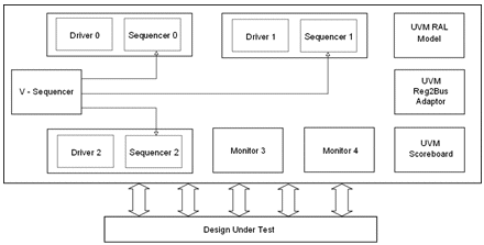
Figure 6: Typical UVM Verification Environment
An asynchronous design uses clocks with different clock ratio combinations which are a result of the different clock domains interfacing with each other. Hence it is essential to verify the design with various combinations of clock ratios and clock skews. Changes in testbench, when a design changes from Sync to Async, depends lot on how you had architect your testbench from start. If it already had an interface for each clock domain then it would be very easy to modify the testbench by just changing the clock sources at interface clocking block (See Fig 8.) but if testbench designer has architected the testbench assuming all clocks are same and synchronous then one might have to go through the trouble of partitioning the testbench based on different clocks (Fig 7).

Figure 7: Verification Environment with single Driver and Monitor

Figure 8: Verification Environment with Separate Driver and Monitor for each interface
The following modules may require update when including the capability for asynchronous clock interfaces in the verification environment:
- Driver: Driver can be as simple as a protocol driver which has inbuilt capability to change output based on baud period and clock source as in DUT. The driver might need proper clock info and some logic to deal with asynchronous clocks. If testbench architecture does not have proper segregation of driver for each clock interface then it is imperative to re-architect the driver. For example, in Fig 8, testbench has driver for each interface so whenever we change the clocks it is just about changing clock to the interface but if we have testbench as shown in Fig 7 then we need to clearly segregate interfaces.
- Monitor: Monitor uses different clocks to generate the response which is used by the response checker. It must be ensured that the response generated by the monitor is separated into appropriate clock domains corresponding to the changes done for clock domain in the DUT in order to correctly check. As in case of the driver, each monitor should be plugged on different interface and we just need to change clock to make testbench asynchronous.
- Response Checker/Scoreboard: Response checker helps check the integrity of data. It basically creates the expected data based on input clocks and checks the data on the output clocks. Hence it is essential to have clear boundary of clock domains inside the checker, for proper response checking. For testbench in Fig 8, it is automatically taken care if we are using clocking blocks of each interface for updating checking for that interface.
The following components of the verification environment will potentially need to be updated:
- Testcases: Testcases need to be modified or added to check functionality under various clock ratios and clock dividers values. Having a random clock ratio and divider values will provide robust checking of an asynchronous design. If a System Verilog based environment is being used, then this can be done by providing the clock ratio and clock skews as parameters which can be randomized. Register read-write tests become important as data may be read from or written to different clock domains which are asynchronous to each other, so proper wait logic in the design will need to be tested. The register read/write driver should have the capability to check this.
- Cover Points: Coverage of checks related to clock ratios and clock skews will need to be added for all existing functional. For e.g.
- Multi Clock Assertions: Multi-Clock Assertions can be added which are used to check signal integrity when crossing from one clock domain to another clock domain. This can be done in addition to clock domain crossing checks on the design. This is a very important aspect which must not be ignored. Without this, potential synchronization issues in the design may never be caught until the silicon is out or they may get caught too late in the design cycle. An example of such an assertion can be
Conclusion:
Design and Verification development is relatively easy when creating an asynchronous design from scratch. However, we are faced with certain challenges and limitations when an existing synchronous design is to be converted into an asynchronous design where the clock ratio between the domains can vary from system to system and where the particular design is used in different configurations. This paper will help designers identify those areas and help in an easier transition from sync to async and verify those key design changes and ensure a good design.
References:
[1] Clifford E.Cumings, Simulation and Synthesis techniques for Asynchronous FIFO Design,http://www.sunburst-design.com/papers/CummingsSNUG2002SJ_FIFO1.pdf
[2] Cadence, Clock Domain Crossing, http://w2.cadence.com/whitepapers/cdc_wp.pdf
About the authors:
-
- Karthik Rao - Design Engineer in Freescale having 3 years experience in Digital IP Design for Serial Interfaces and Signal Processing applications.
- Nitin Goel - Design Engineer in Freescale having 6 years experience in IP and SOC verification
- Prashant Bhargava - System Architect in Freescale having 12+ years of experience in SoC & IP design for automotive and metering applications
转载于:https://www.cnblogs.com/bluefish/archive/2013/06/09/3129435.html
最后
以上就是清新书包最近收集整理的关于Design Transition from Sync to Async: Design and Verification Challenges 的全部内容,更多相关Design内容请搜索靠谱客的其他文章。


发表评论 取消回复