IDDR原语
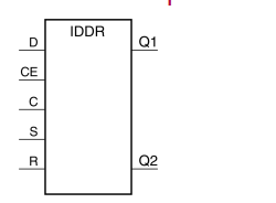
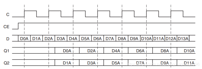
如图所示,IDDR原语的输入输出包括D,CE,C,S,R,Q1,Q2,其中,D为输入的双倍速率的数据,即D在时钟的上升沿和下降沿都会发生切换,一个时钟周期发送2bit数据,CE为时钟使能信号,C为时钟信号,S,R为复位和置位信号,Q1,Q2为单倍速率的输出数据。
IDDR主要有三种工作模式,分别是:OPPOSITE_EDGE, SAME_EDGE,SAME_EDGE_PIPELINED 。
下面分别作一介绍:
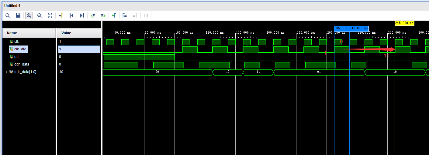
1.OPPOSITE_EDGE
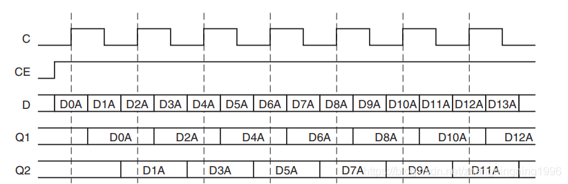
在该模式下,上升沿采样到的数据(如DOA)和下降沿采样到的数据(如D1A),可以在下一个时钟周期的上升沿从Q1,Q2端口读取。
附一张仿真的效果图:
2.SAME_EDGE
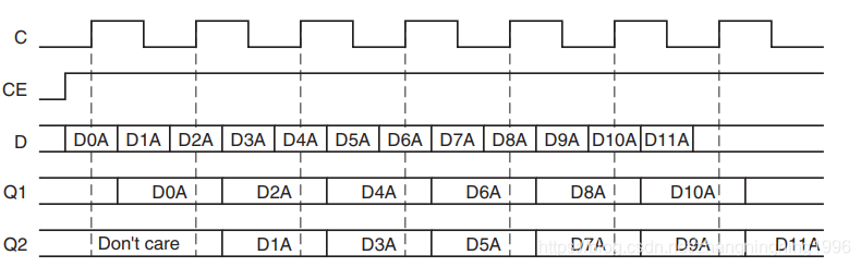
在该模式下,上升沿读取的数据,可以在下一个时钟周期的上升沿从Q1端口读取,而下降沿读取的数据,可以在下下个时钟周期的上升沿从Q2端口读取。
仿真波形如下
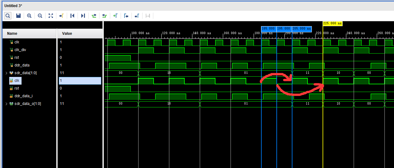
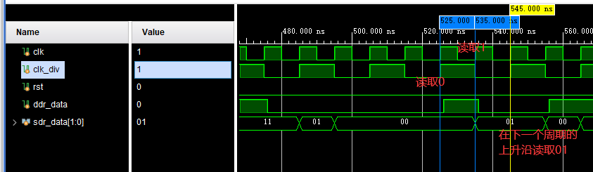
3.SAME_EDGE_PIPELINED
在该模式下,上升沿和下降沿捕获的数据将可以在下下个时钟周期的上升沿从Q1,Q2端口读取。
仿真波形如下:
代码
设计文件
`timescale 1ns / 1ps
//
// Company:
// Engineer:
//
// Create Date: 2021/12/26 19:04:39
// Design Name:
// Module Name: top
// Project Name:
// Target Devices:
// Tool Versions:
// Description:
//
// Dependencies:
//
// Revision:
// Revision 0.01 - File Created
// Additional Comments:
//
//


module top(
input logic clk,
input logic rst,
input logic ddr_data_i,
output logic [1:0] sdr_data_o
    );


//      IDDR     : In order to incorporate this function into the design,
//     Verilog   : the following instance declaration needs to be placed
//    instance   : in the body of the design code.  The instance name
//   declaration : (IDDR_inst) and/or the port declarations within the
//      code     : parenthesis may be changed to properly reference and
//               : connect this function to the design.  Delete or comment
//               : out inputs/outs that are not necessary.

//  <-----Cut code below this line---->

   // IDDR: Input Double Data Rate Input Register with Set, Reset
   //       and Clock Enable.
   //       Artix-7
   // Xilinx HDL Language Template, version 2019.2

IDDR #(
    .DDR_CLK_EDGE("SAME_EDGE_PIPELINED"), // "OPPOSITE_EDGE", "SAME_EDGE"
                                    //    or "SAME_EDGE_PIPELINED"
    .INIT_Q1(1'b0), // Initial value of Q1: 1'b0 or 1'b1
    .INIT_Q2(1'b0), // Initial value of Q2: 1'b0 or 1'b1
    .SRTYPE("SYNC") // Set/Reset type: "SYNC" or "ASYNC"
) IDDR_inst (
    .Q1(sdr_data_o[1]), // 1-bit output for positive edge of clock
    .Q2(sdr_data_o[0]), // 1-bit output for negative edge of clock
    .C(clk),   // 1-bit clock input
    .CE(1'b1), // 1-bit clock enable input
    .D(ddr_data_i),   // 1-bit DDR data input
    .R(1'b0),   // 1-bit reset
    .S(rst)    // 1-bit set
);
// End of IDDR_inst instantiation


endmodule
测试平台
`timescale 1ns / 1ps
//
// Company:
// Engineer:
//
// Create Date: 2021/12/26 19:18:01
// Design Name:
// Module Name: test_tb
// Project Name:
// Target Devices:
// Tool Versions:
// Description:
//
// Dependencies:
//
// Revision:
// Revision 0.01 - File Created
// Additional Comments:
//
//


module test_tb(

    );

logic clk;
logic clk_div;
logic rst;
logic ddr_data;
logic [1:0] sdr_data;
//clk
initial begin
    clk=0;
    forever begin
        #5 clk=~clk;
    end
end
//clk_div
always_ff@(posedge clk,posedge rst)
if(rst)
    clk_div<=0;
else
    clk_div<=~clk_div;
//rst
initial begin
    rst=1;
    #100
    rst=0;
end
//ddr_data
always_ff@(posedge clk)
begin
    ddr_data<=#1 $random%2;
end
//inst
top U(
.clk(clk_div),
.rst(rst),
.ddr_data_i(ddr_data),
.sdr_data_o(sdr_data)
);
endmodule
ODDR原语
如图,ODDR和IDDR相反,它的功能是将单倍速率的数据转化成双倍速率的数据,分为OPPOSITE_EDGE模式和SAME_EDGE模式
1.OPPOSITE_EDGE模式
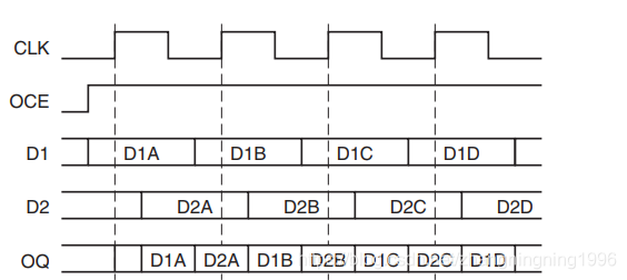
该模式下,上升沿读取D1数据,并在时钟周期的前半个周期输出,下降沿读取D2数据,并在时钟周期的后半个周期输出。
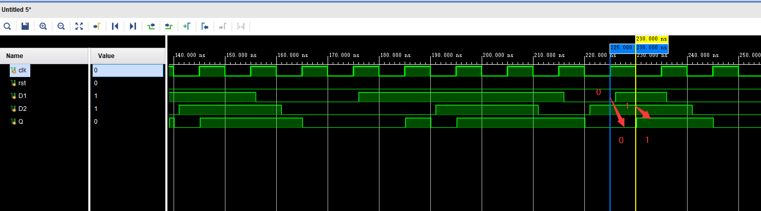
仿真波形如下
2.SAME_EDGE模式
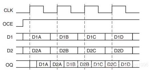
该模式下,时钟周期的上升沿同时读取D1,D2数据,并在前半个时钟周期输出D1,后半个时钟周期输出D2。
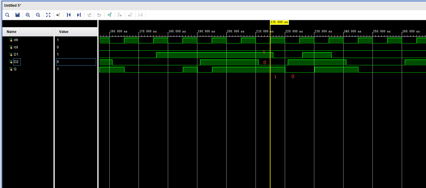
仿真波形如下:
代码
设计文件
`timescale 1ns / 1ps
//
// Company:
// Engineer:
//
// Create Date: 2021/12/26 19:04:39
// Design Name:
// Module Name: top
// Project Name:
// Target Devices:
// Tool Versions:
// Description:
//
// Dependencies:
//
// Revision:
// Revision 0.01 - File Created
// Additional Comments:
//
//


module top(
input logic clk,
input logic rst,
input logic D1,
input logic D2,
output logic Q
    );


//      ODDR     : In order to incorporate this function into the design,
//     Verilog   : the following instance declaration needs to be placed
//    instance   : in the body of the design code.  The instance name
//   declaration : (ODDR_inst) and/or the port declarations within the
//      code     : parenthesis may be changed to properly reference and
//               : connect this function to the design.  Delete or comment
//               : out inputs/outs that are not necessary.

//  <-----Cut code below this line---->

   // ODDR: Output Double Data Rate Output Register with Set, Reset
   //       and Clock Enable.
   //       Artix-7
   // Xilinx HDL Language Template, version 2019.2

ODDR #(
    .DDR_CLK_EDGE("SAME_EDGE"), // "OPPOSITE_EDGE" or "SAME_EDGE"
    .INIT(1'b0),    // Initial value of Q: 1'b0 or 1'b1
    .SRTYPE("SYNC") // Set/Reset type: "SYNC" or "ASYNC"
) ODDR_inst (
    .Q(Q),   // 1-bit DDR output
    .C(clk),   // 1-bit clock input
    .CE(1'b1), // 1-bit clock enable input
    .D1(D1), // 1-bit data input (positive edge)
    .D2(D2), // 1-bit data input (negative edge)
    .R(1'b0),   // 1-bit reset
    .S(rst)    // 1-bit set
);

// End of ODDR_inst instantiation


endmodule
测试文件
`timescale 1ns / 1ps
//
// Company:
// Engineer:
//
// Create Date: 2021/12/26 19:18:01
// Design Name:
// Module Name: test_tb
// Project Name:
// Target Devices:
// Tool Versions:
// Description:
//
// Dependencies:
//
// Revision:
// Revision 0.01 - File Created
// Additional Comments:
//
//


module test_tb(

    );

logic clk;
logic clk_n;
logic clk_div;
logic rst;
logic D1,D2;
logic Q;
//clk
initial begin
    clk=0;
    forever begin
        #5 clk=~clk;
    end
end
//clk_n
assign clk_n=~clk;
//clk_div
always_ff@(posedge clk,posedge rst)
if(rst)
    clk_div<=0;
else
    clk_div<=~clk_div;
//rst
initial begin
    rst=1;
    #100
    rst=0;
end
//D1
always_ff@(posedge clk)
    D1<=#1 $random%2;
//D2
always_ff@(posedge clk_n)
    D2<=#1 $random%2;
//
top U(
.clk(clk),
.rst(rst),
.D1(D1),
.D2(D2),
.Q(Q)
);
endmodule
最后
以上就是干净咖啡豆最近收集整理的关于Xilinx IDDR与ODDR原语的使用IDDR原语ODDR原语的全部内容,更多相关Xilinx内容请搜索靠谱客的其他文章。
本图文内容来源于网友提供,作为学习参考使用,或来自网络收集整理,版权属于原作者所有。


发表评论 取消回复