D触发器
创建单个 D 触发器。
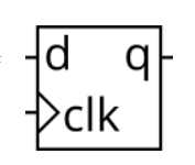
D触发器是一种存储位并在时钟信号(通常)正沿处定期更新的电路。D 触发器在使用时钟始终块时由逻辑合成器创建。AD触发器是“组合逻辑块后跟触发器”的最简单形式,其中组合逻辑部分只是一条线。
Module Declaration
module top_module (
    input clk,    // Clocks are used in sequential circuits
    input d,
    output reg q );
答案:
module top_module (
    input clk,    // Clocks are used in sequential circuits
    input d,
    output reg q );//
    always @(posedge clk)begin
        q <= d ;
    end
endmodule
8个 D触发器
创建 8 个 D 触发器。所有 DFF 都应由clk 的上升沿触发。
Module Declaration
module top_module (
    input clk,
    input [7:0] d,
    output [7:0] q
);
答案:
module top_module (
    input clk,
    input [7:0] d,
    output [7:0] q
);
	always @(posedge clk)begin
        q <= d ;
    end
endmodule
8个带同步复位的D触发器
创建具有高电平有效同步复位的 8 个 D 触发器。所有 DFF 都应由clk 的上升沿触发。
Module Declaration
module top_module (
    input clk,
    input reset,            // Synchronous reset
    input [7:0] d,
    output [7:0] q
);
答案:
module top_module (
    input clk,
    input reset,            // Synchronous reset
    input [7:0] d,
    output [7:0] q
);
	always @(posedge clk)begin
        if(reset == 1)
            q <= 0 ;
        else
        	q <= d ;
    end
endmodule
8个带复位值的D触发器
创建具有高电平有效同步复位的 8 个 D 触发器。触发器必须重置为 0x34 而不是零。所有的DFF应由被触发负的边缘CLK。
Module Declaration
module top_module (
    input clk,
    input reset,            // Synchronous reset
    input [7:0] d,
    output [7:0] q
);
答案:
module top_module (
    input clk,
    input reset,
    input [7:0] d,
    output [7:0] q
);
    always @(negedge clk)begin
        if(reset == 1)
            q <= 8'h34;
        else
        	q <= d ;
    end
endmodule
8个带异步复位的D触发器
创建具有高电平有效异步复位的 8 个 D 触发器。所有 DFF 都应由clk 的上升沿触发。
Module Declaration
module top_module (
    input clk,
    input areset,   // active high asynchronous reset
    input [7:0] d,
    output [7:0] q
);
答案:
module top_module (
    input clk,
    input areset,   // active high asynchronous reset
    input [7:0] d,
    output [7:0] q
);
    always @(posedge clk or posedge areset)begin
        if(areset == 1)
            q <= 8'h00;
        else
        	q <= d ;
    end
endmodule
16 个 D 触发器
创建 16 个 D 触发器。有时只修改一组触发器的一部分很有用。字节使能输入控制是否应在该周期写入 16 个寄存器的每个字节。byteena[1]控制高字节d[15:8],而byteena[0]控制低字节d[7:0]。
resetn是一个同步的、低电平有效的复位。
所有 DFF 都应由clk 的上升沿触发。
Module Declaration
module top_module (
    input clk,
    input resetn,
    input [1:0] byteena,
    input [15:0] d,
    output [15:0] q
);
答案:
module top_module (
    input clk,
    input resetn,
    input [1:0] byteena,
    input [15:0] d,
    output [15:0] q
);
    always @(posedge clk)begin
        if(resetn == 0)
            q <= 8'h00;
        else if(byteena [1] ==1 && byteena [0] ==1)
            q <= d;
        else if(byteena [1] ==1)
            q[15:8]<= d[15:8];
        else if(byteena [0] ==1)
            q[7:0]<= d[7:0];
        else
            q <= q;
    end
endmodule
D 锁存器
实现以下电路:
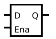
请注意,这是一个闩锁,因此预计会出现有关推断闩锁的 Quartus 警告。
Module Declaration
module top_module (
    input d,
    input ena,
    output q);
答案:
module top_module (
    input d,
    input ena,
    output q);
	always @(ena)begin
        if(ena == 1)
        	q = d ;
    end
endmodule
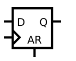
DFF
实现以下电路:
Module Declaration
module top_module (
    input clk,
    input d,
    input ar,   // asynchronous reset
    output q);
答案:
module top_module (
    input clk,
    input d,
    input ar,   // asynchronous reset
    output q);
    always @(posedge clk or posedge ar)begin
        if(ar == 1)begin
           q<=0;
        end
        else begin
           q<=d;
        end
    end
endmodule
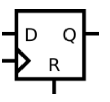
DFF1
实现以下电路:
Module Declaration
module top_module (
    input clk,
    input d,
    input r,   // synchronous reset
    output q);
答案:
module top_module (
    input clk,
    input d,
    input r,   // synchronous reset
    output q);
	always @(posedge clk)begin
        if(r == 1)begin
           q<=0;
        end
        else begin
           q<=d;
        end
    end
endmodule
DFF+gate
Module Declaration
module top_module (
    input clk,
    input in,
    output out);
答案:
module top_module (
    input clk,
    input in,
    output out);
	always @(posedge clk)begin
    	out<=in^out;
    end
endmodule
MAX and DFF
考虑下面的时序电路:
假设您要为该电路实现分层 Verilog 代码,使用其中包含触发器和多路复用器的子模块的三个实例。为此子模块编写一个名为top_module的 Verilog 模块(包含一个触发器和多路复用器)。
Module Declaration
module top_module (
	input clk,
	input L,
	input r_in,
	input q_in,
	output reg Q);
答案:
module top_module (
	input clk,
	input L,
	input r_in,
	input q_in,
	output reg Q);

    always @(posedge clk)begin
        if(L==0)begin
            Q <= q_in;
        end
        else begin
           Q <= r_in;
        end
    end
endmodule
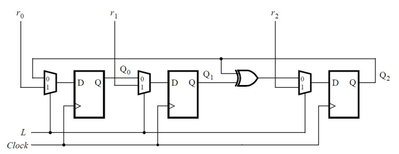
MAX and DFF1
考虑如下所示的n位移位寄存器电路:
为该电路的一个阶段编写一个名为 top_module 的 Verilog 模块,包括触发器和多路复用器。
Module Declaration
module top_module (
    input clk,
    input w, R, E, L,
    output Q
);
答案:
module top_module (
    input clk,
    input w, R, E, L,
    output Q
);
    wire E_in = (E==1)?w:Q;
    always @(posedge clk)begin
        if(L==1)begin
            Q <= R;
        end
        else begin
            Q <= E_in;
        end
    end
endmodule
DFF and gates
给定如图所示的有限状态机电路,假设 D 触发器在机器启动之前初始复位为零。
建立这个电路。
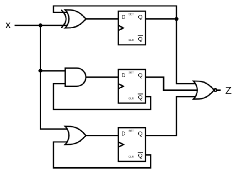
Module Declaration
module top_module (
    input clk,
    input x,
    output z
);
答案:
module top_module (
    input clk,
    input x,
    output z
);
    assign z = !(Q0|Q1|Q2);
    reg Q0;
    always @(posedge clk)begin
    	Q0 <= x^Q0;
    end
    reg Q1;
    always @(posedge clk)begin
    	Q1 <= x&!Q1;
    end
    reg Q2;
    always @(posedge clk)begin
    	Q2 <= x|!Q2;
    end
endmodule
从真值表创建电路
JK 触发器具有以下真值表。仅使用 D 型触发器和门实现 JK 触发器。注:Qold 是时钟正沿前 D 触发器的输出。
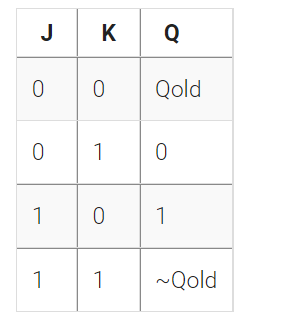
Module Declaration
module top_module (
    input clk,
    input j,
    input k,
    output Q);
答案:
module top_module (
    input clk,
    input j,
    input k,
    output Q);
    always @(posedge clk)begin
        if({j,k}==2'b00)begin
           Q<=Q;
        end
        else if({j,k}==2'b01)begin
           Q<=0;
        end
        else if({j,k}==2'b10)begin
           Q<=1;
        end
        else begin
           Q<=!Q;
        end
    end
endmodule
边沿检测(上升沿)
对于 8 位向量中的每一位,检测输入信号何时从一个时钟周期内的 0 变为下一个时钟周期的 1(类似于正沿检测)。输出位应在发生 0 到 1 转换后的周期设置。
这里有一些例子。为了清楚起见,分别显示了 in[1] 和 pedge[1]。
Module Declaration
module top_module (
    input clk,
    input [7:0] in,
    output [7:0] pedge
);
答案:
module top_module (
    input clk,
    input [7:0] in,
    output [7:0] pedge
);
    reg [7:0] in_d1,in_d2;
    assign pedge = in_d1&(~in_d2);

	always @(posedge clk)begin
        in_d1 <= in;
        in_d2 <= in_d1;
    end
endmodule
边沿检测(双沿检测)
对于 8 位向量中的每一位,检测输入信号何时从一个时钟周期变为下一个时钟周期(检测任何边沿)。输出位应在发生 0 到 1 转换后的周期设置。
这里有一些例子。为了清楚起见,分别显示了 in[1] 和 anyedge[1]
Module Declaration
module top_module (
    input clk,
    input [7:0] in,
    output [7:0] anyedge
);
答案:
module top_module (
    input clk,
    input [7:0] in,
    output [7:0] anyedge
);
	reg [7:0] in_d1,in_d2;
    assign anyedge = (in_d1&(~in_d2)) | ((~in_d1)& in_d2);

	always @(posedge clk)begin
        in_d1 <= in;
        in_d2 <= in_d1;
    end
endmodule
边沿捕获
对于 32 位向量中的每一位,当输入信号在一个时钟周期内从 1 变为下一个时钟周期时捕获。“捕获”表示输出将保持为 1,直到寄存器复位(同步复位)。
每个输出位的行为就像一个 SR 触发器:输出位应在 1 到 0 转换发生后的周期设置(为 1)。当复位为高电平时,输出位应在时钟正沿复位(为 0)。如果上述两个事件同时发生,则重置优先。在下面示例波形的最后 4 个周期中,‘reset’ 事件比 ‘set’ 事件早一个周期发生,因此这里没有冲突。
在下面的示例波形中,为清楚起见,再次分别显示了复位、输入 [1] 和输出 [1]。
Module Declaration
module top_module (
    input clk,
    input reset,
    input [31:0] in,
    output [31:0] out
);
答案:
module top_module (
    input clk,
    input reset,
    input [31:0] in,
    output [31:0] out
);
	reg [31:0] in_d1,in_d2;
	always @(posedge clk)begin
        in_d1 <= in;
        in_d2 <= in_d1;
    end

	always @(posedge clk)begin
        if(reset==1)
            out <= 0;
        else if((|((~in) & in_d1)) == 1)
            out <= (~in) & in_d1 | out;
        else
            out <= out;
    end
endmodule
双沿触发器
您熟悉在时钟的正沿或时钟的负沿触发的触发器。双边沿触发触发器在时钟的两个边沿触发。但是,FPGA 没有双边沿触发的触发器,并且始终不接受@(posedge clk 或 negedge clk)作为合法的敏感列表。
构建一个功能类似于双边沿触发触发器的电路:
Module Declaration
module top_module (
    input clk,
    input d,
    output q
);
答案:
module top_module (
    input clk,
    input d,
    output q
);
    reg q1,q2;
    assign q = (clk)?q1:q2;
    always @ (posedge clk)begin
    	q1 <= d;
    end
    always @ (negedge clk)begin
    	q2 <= d;
    end
endmodule
最后
以上就是强健胡萝卜最近收集整理的关于HDLBits练习汇总-10-时序逻辑设计测试--锁存器和触发器D触发器8个 D触发器8个带同步复位的D触发器8个带复位值的D触发器8个带异步复位的D触发器16 个 D 触发器D 锁存器DFFDFF1DFF+gateMAX and DFFMAX and DFF1DFF and gates从真值表创建电路边沿检测(上升沿)边沿检测(双沿检测)边沿捕获双沿触发器的全部内容,更多相关HDLBits练习汇总-10-时序逻辑设计测试--锁存器和触发器D触发器8个内容请搜索靠谱客的其他文章。


发表评论 取消回复