为了方便做笔记,从移位寄存器(Shift Registers)这章开始按章节做记录。
1. 4-bit Shift Registers
题目:
Build a 4-bit shift register (right shift), with asynchronous reset, synchronous load, and enable.
- areset: Resets shift register to zero.
- load: Loads shift register with data[3:0] instead of shifting.
- ena: Shift right (q[3] becomes zero, q[0] is shifted out and disappears).
- q: The contents of the shift register.
If both the load and ena inputs are asserted (1), the load input has higher priority.
思路:
设计一个4位逻辑移位寄存器(右移),寄存器具有异步复位,同步加载和使能。
复位:寄存器置为0。
加载:加载data[3:0]到寄存器中。
使能:寄存器右移。
q:移位寄存器。
需要注意的是,题目要求当加载和使能同时为高电平时,优先对数据进行加载。
代码:
module top_module(
    input clk,
    input areset,  // async active-high reset to zero
    input load,
    input ena,
    input [3:0] data,
    output reg [3:0] q);
    always@(posedge clk, posedge areset) begin
        if(areset)
            q<=0;
        else if(load)
            q <= data;
        else if(ena) begin
            q[0]<=q[1];
            q[1]<=q[2];
            q[2]<=q[3];
            q[3]<=0;
// q <=q[3:1];
        end
    end
endmodule
2.Left/right rotator
题目:
Build a 100-bit left/right rotator, with synchronous load and left/right enable. A rotator shifts-in the shifted-out bit from the other end of the register, unlike a shifter that discards the shifted-out bit and shifts in a zero. If enabled, a rotator rotates the bits around and does not modify/discard them.
- load: Loads shift register with data[99:0] instead of rotating.
- ena[1:0]: Chooses whether and which direction to rotate.
- 2'b01 rotates right by one bit
- 2'b10 rotates left by one bit
- 2'b00 and 2'b11 do not rotate.
- q: The contents of the rotator.
思路:
顾名思义是一个可控制左移/右移的循环移位寄存器,同步加载。与题1不同的是,移位后的数据将会翻折到另一端而不是置0。
题中使能端ena[1:0]控制寄存器是否左移/右移。
代码:
module top_module(
    input clk,
    input load,
    input [1:0] ena,
    input [99:0] data,
    output reg [99:0] q);
    always@(posedge clk) begin
        if(load)
            q <= data;
        else begin
            case(ena)
                2'b01: q <= {q[0],q[99:1]};
                2'b10: q <= {q[98:0],q[99]};
                default: q <= q;
            endcase
        end
    end
endmodule
3.Left/right arithmetic shift by 1 0r 8
题目:
Build a 64-bit arithmetic shift register, with synchronous load. The shifter can shift both left and right, and by 1 or 8 bit positions, selected by amount.
An arithmetic right shift shifts in the sign bit of the number in the shift register (q[63] in this case) instead of zero as done by a logical right shift. Another way of thinking about an arithmetic right shift is that it assumes the number being shifted is signed and preserves the sign, so that arithmetic right shift divides a signed number by a power of two.
There is no difference between logical and arithmetic left shifts.
- load: Loads shift register with data[63:0] instead of shifting.
- ena: Chooses whether to shift.
- amount: Chooses which direction and how much to shift.
- 2'b00: shift left by 1 bit.
- 2'b01: shift left by 8 bits.
- 2'b10: shift right by 1 bit.
- 2'b11: shift right by 8 bits.
- q: The contents of the shifter.
思路:
本题要求设计一个可实现左移/右移功能的算数移位寄存器,与逻辑移位寄存器不同的地方在于,有符号数需要考虑算数右移。
对于无符号数,算数移位寄存器与逻辑移位寄存器实现方法一致。
对于有符号数,算数左移与逻辑左移一致,移位后补0;算数右移与逻辑右移不同,算数右移左侧需补充符号位而非0。
代码:
module top_module(
    input clk,
    input load,
    input ena,
    input [1:0] amount,
    input [63:0] data,
    output reg [63:0] q);
    always@(posedge clk) begin
        if(load)
            q <= data;
        else if(ena)
        begin
            case(amount)
                2'b00: q <= {q[62:0],1'b0};
                2'b01: q <= {q[55:0],{8{1'b0}}};
                2'b10: q <= {q[63],q[63:1]};
                2'b11: q <= {{8{q[63]}},q[63:8]};
            endcase
        end
    end
endmodule
4. 5bits LFSR
题目:
A linear feedback shift register is a shift register usually with a few XOR gates to produce the next state of the shift register. A Galois LFSR is one particular arrangement where bit positions with a "tap" are XORed with the output bit to produce its next value, while bit positions without a tap shift. If the taps positions are carefully chosen, the LFSR can be made to be "maximum-length". A maximum-length LFSR of n bits cycles through 2n-1 states before repeating (the all-zero state is never reached).
The following diagram shows a 5-bit maximal-length Galois LFSR with taps at bit positions 5 and 3. (Tap positions are usually numbered starting from 1). Note that I drew the XOR gate at position 5 for consistency, but one of the XOR gate inputs is 0.

思路:
题目提供了一个线性反馈移位寄存器的电路图,这一个带有若干个XOR门的移位寄存器,将带有抽头的位置与输出位进行异或运算来产生下一个值。
代码:
module top_module(
    input clk,
    input reset,    // Active-high synchronous reset to 5'h1
    output [4:0] q
);
    always@(posedge clk) begin
        if(reset)
            q <= 5'h1;
        else begin
            q[4] <= q[0]^0;
            q[3] <= q[4];
            q[2] <= q[3]^q[0];
            q[1] <= q[2];
            q[0] <= q[1];
        end
    end
endmodule
官方解法:
module top_module(
	input clk,
	input reset,
	output reg [4:0] q);

	reg [4:0] q_next;		// q_next is not a register

	// Convenience: Create a combinational block of logic that computes
	// what the next value should be. For shorter code, I first shift
	// all of the values and then override the two bit positions that have taps.
	// A logic synthesizer creates a circuit that behaves as if the code were
	// executed sequentially, so later assignments override earlier ones.
	// Combinational always block: Use blocking assignments.
	always @(*) begin
		q_next = q[4:1];	// Shift all the bits. This is incorrect for q_next[4] and q_next[2]
		q_next[4] = q[0];	// Give q_next[4] and q_next[2] their correct assignments
		q_next[2] = q[3] ^ q[0];
	end


	// This is just a set of DFFs. I chose to compute the connections between the
	// DFFs above in its own combinational always block, but you can combine them if you wish.
	// You'll get the same circuit either way.
	// Edge-triggered always block: Use non-blocking assignments.
	always @(posedge clk) begin
		if (reset)
			q <= 5'h1;
		else
			q <= q_next;
	end

endmodule
5. 3-bit LFSR
题目:
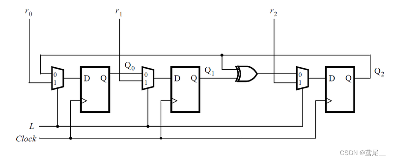
Write the Verilog code for this sequential circuit (Submodules are ok, but the top-level must be named top_module). Assume that you are going to implement the circuit on the DE1-SoC board. Connect the R inputs to the SW switches, connect Clock to KEY[0], and L to KEY[1]. Connect the Q outputs to the red lights LEDR.

为题目所给的时序逻辑电路写一段代码。其中输入R为SW,时钟信号为KEY[0],选择器判别信号为KEY[1],输出Q为LEDR。
思路:
将时序和组合分别写在两个模块内,一个实现触发器功能,一个实现选择器功能。
代码:
module top_module (
	input [2:0] SW,      // R
	input [1:0] KEY,     // L and clk
	output [2:0] LEDR);  // Q
    reg [2:0] temp;
    always@(*) begin
        temp[0] = KEY[1] ? SW[0] : LEDR[2];
        temp[1] = KEY[1] ? SW[1] : LEDR[0];
        temp[2] = KEY[1] ? SW[2] : (LEDR[2]^LEDR[1]);
    end
    always@(posedge KEY[0]) begin
        LEDR[2] <= temp[2];
        LEDR[1] <= temp[1];
        LEDR[0] <= temp[0];
    end
endmodule
6. 32-bit LFSR
题目:
Build a 32-bit Galois LFSR with taps at bit positions 32, 22, 2, and 1.
This is long enough that you'd want to use vectors, not 32 instantiations of DFFs.
思路:
设计一个32位的LFSR,抽头位置在32,22,2,1。与LFSR5思路一致,只是寄存器位数较大,因此题目提示我们不要实例化32个触发器。
可以直接对Q(即qnext)进行移位运算,再对抽头位置逐一进行修正。
代码:
module top_module(
    input clk,
    input reset,    // Active-high synchronous reset to 32'h1
    output [31:0] q
);
    reg [31:0] Q;
    always@(*) begin
        Q = {q[0],q[31:1]};
        Q[21] = q[22]^q[0];
        Q[1] = q[2]^q[0];
        Q[0] = q[1]^q[0];
    end
    always@(posedge clk) begin
        if(reset)
            q <= 32'h1;
    	else
            q <= Q;
    end
endmodule
7.Shift register(Exams/m2014 q4k)
题目:
Implement the following circuit:

思路:
实现上述时序电路,包含4个DFF,1个输入in,1个输入out,所有触发器具有相同输入的时钟信号以及同步复位信号resetn(低电平有效)。
考虑创建一个寄存器Q来存储触发器的输出值。
代码:
module top_module (
    input clk,
    input resetn,   // synchronous reset
    input in,
    output out);
    reg[3:1] Q;
    always@(posedge clk) begin
        if(!resetn) begin
            Q <= 0;
        	out <=0;
        end
        else begin
            Q[1] <= in;
            Q[2] <= Q[1];
            Q[3] <= Q[2];
            out <= Q[3];
        end
    end
endmodule
官方解法:
module top_module (
	input clk,
	input resetn,
	input in,
	output out
);

	reg [3:0] sr;

	// Create a shift register named sr. It shifts in "in".
	always @(posedge clk) begin
		if (~resetn)		// Synchronous active-low reset
			sr <= 0;
		else
			sr <= {sr[2:0], in};
	end

	assign out = sr[3];		// Output the final bit (sr[3])

endmodule
8.Shift register(Exams/2014 q4b)
题目:
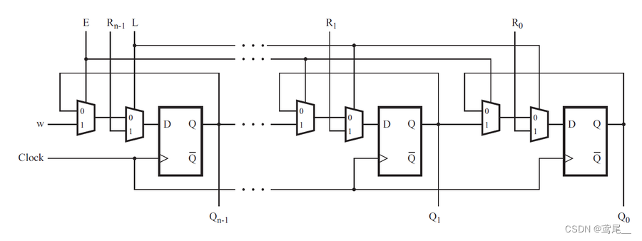
Consider the n-bit shift register circuit shown below:

Write a top-level Verilog module (named top_module) for the shift register, assuming that n = 4. Instantiate four copies of your MUXDFF subcircuit in your top-level module. Assume that you are going to implement the circuit on the DE2 board.
- Connect the R inputs to the SW switches,
- clk to KEY[0],
- E to KEY[1],
- L to KEY[2], and
- w to KEY[3].
- Connect the outputs to the red lights LEDR[3:0].
(Reuse your MUXDFF from exams/2014_q4a.)
思路:
题目给出了一个n-bit移位寄存器电路,要求我们按照该电路的模式设计一个4-bit移位寄存器。
题目要求实例化4个由“两个选择器+单个触发器“”组成的MUXDFF来完成电路设计。
代码:
module top_module (
    input [3:0] SW,
    input [3:0] KEY,
    output [3:0] LEDR
); //
    MUXDFF u4(
        .clk(KEY[0]),
        .E	(KEY[1]),
        .R	(SW[3]),
        .L	(KEY[2]),
        .w	(KEY[3]),
        .Q	(LEDR[3])
    );
	MUXDFF u3(
        .clk(KEY[0]),
        .E	(KEY[1]),
        .R	(SW[2]),
        .L	(KEY[2]),
        .w	(LEDR[3]),
        .Q	(LEDR[2])
    );
    MUXDFF u2(
        .clk(KEY[0]),
        .E	(KEY[1]),
        .R	(SW[1]),
        .L	(KEY[2]),
        .w	(LEDR[2]),
        .Q	(LEDR[1])
    );
    MUXDFF u1(
        .clk(KEY[0]),
        .E	(KEY[1]),
        .R	(SW[0]),
        .L	(KEY[2]),
        .w	(LEDR[1]),
        .Q	(LEDR[0])
    );
endmodule

module MUXDFF (
    input clk,
    input E,
    input R,
    input L,
    input w,
    output Q
);
    wire t1,t2;
    always@(*) begin
        t1 = E ? w:Q;
        t2 = L ? R:t1;
    end
    always@(posedge clk) begin
        Q <= t2;
    end
endmodule
9. 3-input LUT(Exams/ece241 2013 q12)
题目:
In this question, you will design a circuit for an 8x1 memory, where writing to the memory is accomplished by shifting-in bits, and reading is "random access", as in a typical RAM. You will then use the circuit to realize a 3-input logic function.
First, create an 8-bit shift register with 8 D-type flip-flops. Label the flip-flop outputs from Q[0]...Q[7]. The shift register input should be called S, which feeds the input of Q[0] (MSB is shifted in first). The enable input controls whether to shift. Then, extend the circuit to have 3 additional inputs A,B,C and an output Z. The circuit's behaviour should be as follows: when ABC is 000, Z=Q[0], when ABC is 001, Z=Q[1], and so on. Your circuit should contain ONLY the 8-bit shift register, and multiplexers. (Aside: this circuit is called a 3-input look-up-table (LUT)).
思路:
用8个触发器和1个3输入单输出的选择器设计一个3输入的查找表。
触发器输出Q[7:0]可以用向量完成,这样就不需要实例化8个D触发器。
查找表部分,因为只是一个3-input的查找表,直接用case枚举了所有可能,实际上在设计一个n-input的查找表时,代码的第一个always块部分应该直接用Z=Q[{A,B,C}]代替。
代码:
module top_module (
    input clk,
    input enable,
    input S,
    input A, B, C,
    output Z );
    reg [7:0] Q;
    always@(*) begin
            case({A,B,C})
                3'b000: Z = Q[0];
                3'b001: Z = Q[1];
                3'b010: Z = Q[2];
                3'b011: Z = Q[3];
                3'b100: Z = Q[4];
                3'b101: Z = Q[5];
                3'b110: Z = Q[6];
                3'b111: Z = Q[7];
            endcase
    end
    always@(posedge clk) begin
        if(enable)
            Q <= {Q[6:0],S};
        else
            Q <= Q;
    end
endmodule
最后
以上就是隐形鞋子最近收集整理的关于HDLBits学习笔记——移位寄存器的全部内容,更多相关HDLBits学习笔记——移位寄存器内容请搜索靠谱客的其他文章。


发表评论 取消回复