文章目录
- Sequential Logic
- Latches and Flip-Flops
- D flip-flop
- D flip-flops
- DFF with reset
- DFF with reset value
- DFF with asynchronous reset
- DFF with byte enable
- D Latch
- DFF_1
- DFF_2
- DFF+gate
- MUX and DFF_1
- MUX and DFF_2
- DFFs and gates
- Create circuit from truth table
- Detect am edge
- Detect both edges
- Edge capture register
- Dual-edge triggered flip-flop
- Counters
- Four-bit binary counter
- Decade counter
- Decade counter again
- Slow decade counter
- Counter 1-12
- Counter 1000
- 4-digit decimal counter
- 12-hour clock
- Shift Registers
- 4-bit shift register
- Left/right rotator
- Left/right arithmetic shift by 1 or 8
- 5-bit LFSR
- 3-bit LFSR
- 32-bit LFSR
- Shift register_1
- Shift register_2
- 3-input LUT
- More Circuits
- Rule 90
- Rule 110
- Conway's Game of Life 16x16
Sequential Logic
Latches and Flip-Flops
D flip-flop
-
Problem Statement
Create a single D flip-flop.
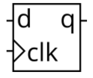
问题示意图(转自HDLBits) -
Code Block
module top_module ( input clk, // Clocks are used in sequential circuits input d, output reg q );// always @(posedge clk) begin q <= d; //时序语句中常用非阻塞性语句 end endmodule -
Key Pointas
D触发器有边缘触发和电平触发两种,常用的是上升沿触发。在时钟上升沿触发以后,次态就等于触发前D的状态,而没触发时状态保持不变,有阻塞的作用。
D触发器状态方程为
Q n + 1 = D Q_{n+1} = D Qn+1=D
D触发器的功能表为
D D D C L K CLK CLK Q n Q_n Qn Q n + 1 Q_{n+1} Qn+1 0 时钟上升沿 1 0 1 时钟上升沿 0 1 X 0 Q n − 1 Q_{n-1} Qn−1 Q n Q_{n} Qn X 1 Q n − 1 Q_{n-1} Qn−1 Q n Q_{n} Qn 注:
在组合逻辑always @(*)中,不管里边用 = 还是 <= ,都是阻塞的效果。
在时序逻辑always@(posedge clk or negedge clk)中,用 = 和 <= ,是有效果的,D触发器结合一些组合逻辑,而使用非阻塞时则为流水线结构,可以构成多个触发器结合的效果。效果示例如下:
module top_module (
    input clk,
    input din,
    output reg out1,out2 );

    always @(posedge clk) begin
        out1 = din; //使用阻塞性语句
        out2 = out1;
    end

endmodule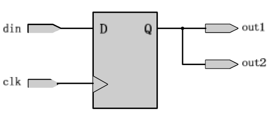
代码电路图(转自西电Verilog课程PPT) module top_module ( input clk, input din, output reg out1,out2 ); always @(posedge clk) begin out1 <= din; //使用非阻塞性语句 out2 <= out1; end endmodule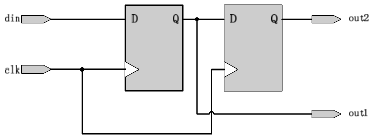
D flip-flops
-
Problem Statement
Create 8 D flip-flops. All DFFs should be triggered by the positive edge of
clk. -
Code Block
module top_module (
    input clk,
    input [7:0] d,
    output [7:0] q
);
    always @(posedge clk)	begin
        q[7:0] <= d[7:0];
    end

endmodule
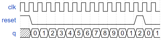
DFF with reset
-
Problem Statement
Create 8 D flip-flops with active high synchronous reset. All DFFs should be triggered by the positive edge of
clk. -
Code Block
module top_module ( input clk, input reset, // Synchronous reset input [7:0] d, output [7:0] q ); always@(posedge clk) begin if(reset) begin q <= 8'b0; end else begin q <= d; end end endmodule -
Key Point
高位同步触发:当reset信号置1后,在时钟上升沿触发。
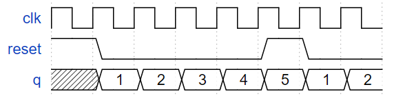
DFF with reset value
-
Problem Statement
Create 8 D flip-flops with active high synchronous reset. The flip-flops must be reset to 0x34 rather than zero. All DFFs should be triggered by the negative edge of
clk. -
Code Block
module top_module (
    input clk,
    input reset,
    input [7:0] d,
    output [7:0] q
);
    always@(negedge clk) begin
        if (reset)	begin
            q <= 8'h34;//0x34
        end
        else	begin
            q <= d;
        end
    end

endmodule
DFF with asynchronous reset
-
Problem Statement
Create 8 D flip-flops with active high asynchronous reset. All DFFs should be triggered by the positive edge of
clk. -
Code Block
module top_module ( input clk, input areset, // active high asynchronous reset input [7:0] d, output [7:0] q ); always @(posedge clk or posedge areset) begin if (areset) begin q <= 8'b0; end else begin q <= d; end end endmodule -
Key Point
高位异步触发:当触发信号置1时,无论clk信号如何马上触发
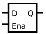
DFF with byte enable
-
Problem Statement
Create 16 D flip-flops. It’s sometimes useful to only modify parts of a group of flip-flops. The byte-enable inputs control whether each byte of the 16 registers should be written to on that cycle.
byteena[1]controls the upper byted[15:8], whilebyteena[0]controls the lower byted[7:0].resetnis a synchronous, active-low reset.All DFFs should be triggered by the positive edge of
clk. -
Code Block
module top_module (
    input clk,
    input resetn,
    input [1:0] byteena,
    input [15:0] d,
    output [15:0] q
);
    always @(posedge clk) begin
        if (resetn) begin //这里不是高位触发
            q[15:8] <= byteena[1] ? d[15:8] : q[15:8];
            q[7:0]  <= byteena[0] ? d[7:0]  : q[7:0];
        end
        else	begin
            q <= 16'b0;
        end
    end
endmodule
D Latch
-
Problem Statement
Implement the following circuit:
-
Code Block
module top_module ( input d, input ena, output q); always@(*) begin if (ena) begin q = d; end end endmodule -
Key Point
锁存器:一般在特定输入脉冲电平下改变状态,其他时候维持电平状态。
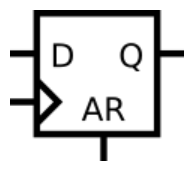
DFF_1
-
Problem Statement
Implement the following circuit:
-
Code Block
module top_module (
    input clk,
    input d,
    input ar,   // asynchronous reset
    output q);
    always @(posedge clk or posedge ar)	begin
        if(ar)	begin
           q <= 1'b0;
        end
        else begin
            q <= d;
        end
    end

endmodule
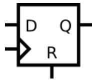
DFF_2
-
Problem Statement
Implement the following circuit:
-
Code Block
module top_module (
    input clk,
    input d,
    input r,   // synchronous reset
    output q);
    always @(posedge clk)	begin
        if(r)	begin
           q <= 1'b0;
        end
        else begin
            q <= d;
        end
    end

endmodule
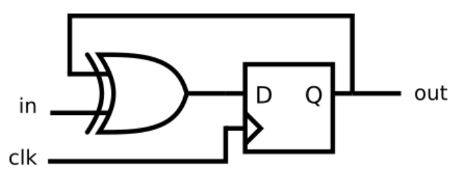
DFF+gate
-
Problem Statement
Implement the following circuit:
-
Code Block
module top_module (
    input clk,
    input in,
    output out);

    always @(posedge clk)	begin
        out <= in^out;
    end

endmodule
MUX and DFF_1
-
Problem Statement
Consider the sequential circuit below:
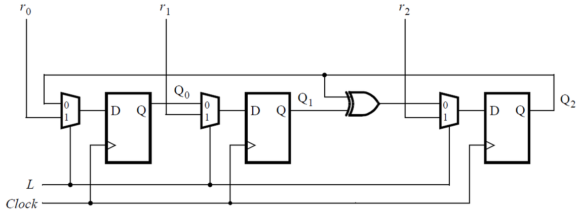
问题示意图(转自HDLBits) Assume that you want to implement hierarchical Verilog code for this circuit, using three instantiations of a submodule that has a flip-flop and multiplexer in it. Write a Verilog module (containing one flip-flop and multiplexer) named
top_modulefor this submodule. -
Code Block
module top_module (
	input clk,
	input L,
	input r_in,
	input q_in,
	output reg Q);

    always @(posedge clk)	begin
        Q <= L ? r_in : q_in ;
    end

endmodule
MUX and DFF_2
-
Problem Statement
Consider the n-bit shift register circuit shown below:
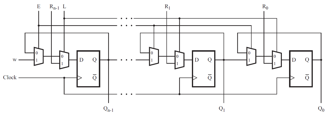
问题示意图(转自HDLBits) -
Code Block
module top_module ( input clk, input w, R, E, L, output Q ); wire temp_x; always @(posedge clk) begin case({E,L}) 2'b00 : Q <= Q; 2'b01,2'b11 : Q <= R; 2'b10 : Q <= w; endcase end endmodule -
Key Point
也可以用另外一种方式实现,如下:
module top_module (
    input clk,
    input w, R, E, L,
    output Q
);
    wire temp_x;
    always @(posedge clk)	begin
        temp_x = E? w : Q;
        Q = L? R : temp_x; //一定要使用阻塞型赋值语句,如果使用非阻塞型赋值语句相当于两个D触发器。

    end

endmodule
DFFs and gates
-
Problem Statment
Given the finite state machine circuit as shown, assume that the D flip-flops are initially reset to zero before the machine begins.
Build this circuit.
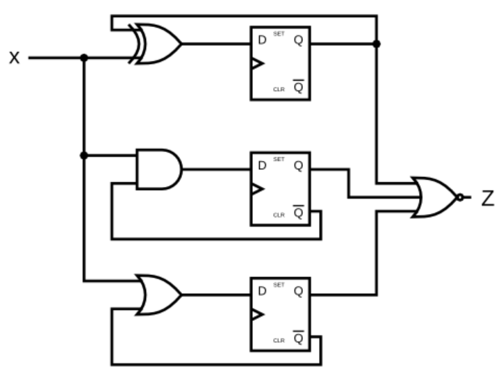
-
Code Block
module top_module (
    input clk,
    input x,
    output z
);
    reg  q_1, q_2, q_3;
    always@(posedge clk)	begin
        q_1 <= q_1 ^ x;
        q_2 <= (~q_2) & x;
        q_3 <= (~q_3) | x;
    end
		assign z = ~(q_1 | q_2 | q_3);
endmodule
Create circuit from truth table
-
Problem Statement
A JK flip-flop has the below truth table. Implement a JK flip-flop with only a D-type flip-flop and gates. Note: Qold is the output of the D flip-flop before the positive clock edge.
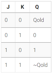
-
Code Block
module top_module (
    input clk,
    input j,
    input k,
    output Q);
    always @(posedge clk)	begin
        case({j,k})
            2'b00 : Q <= Q;
            2'b01 : Q <= 0;
            2'b10 : Q <= 1;
            2'b11 : Q <= ~Q;
        endcase
    end
endmodule
Detect am edge
-
Problem Statement
For each bit in an 8-bit vector, detect when the input signal changes from 0 in one clock cycle to 1 the next (similar to positive edge detection). The output bit should be set the cycle after a 0 to 1 transition occurs.
-
Code Block
module top_module ( input clk, input [7:0] in, output [7:0] pedge ); reg [7:0] temp_in; always @(posedge clk )begin temp_in <= in; pedge <= in & ~temp_in; end endmodule -
Key Point
检测信号上升沿,说明是低电平变高电平。
Detect both edges
-
Problem Statement
For each bit in an 8-bit vector, detect when the input signal changes from one clock cycle to the next (detect any edge). The output bit should be set the cycle after a 0 to 1 transition occurs.
-
Code Block
module top_module ( input clk, input [7:0] in, output [7:0] anyedge ); reg [7:0] temp_in; always@(posedge clk) begin temp_in <= in; anyedge <= temp_in ^ in; end endmodule -
Key Point
检测信号变化只要与上一个信号做异或运算即可。
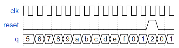
Edge capture register
-
Problem Statement
For each bit in a 32-bit vector, capture when the input signal changes from 1 in one clock cycle to 0 the next. “Capture” means that the output will remain 1 until the register is reset (synchronous reset).
Each output bit behaves like a SR flip-flop: The output bit should be set (to 1) the cycle after a 1 to 0 transition occurs. The output bit should be reset (to 0) at the positive clock edge when reset is high. If both of the above events occur at the same time, reset has precedence. In the last 4 cycles of the example waveform below, the ‘reset’ event occurs one cycle earlier than the ‘set’ event, so there is no conflict here.
-
Code Block
module top_module ( input clk, input reset, input [31:0] in, output [31:0] out ); reg [31:0] temp_in; integer i; always@(posedge clk) begin temp_in <= in; //记录in上一个状态位 for(i=0; i<32; i++) begin case({temp_in[i] & (~in[i]), reset}) //下降沿检测位和reset位,基本功能类似RS触发器 2'b00 : out[i] <= out[i]; //保持不变 2'b01, 2'b11 : out[i] <= 1'b0; //reset置1且具有优先级,则输出位 置0 2'b10 : out[i] <= 1'b1; //下降沿检测触发,输出位 置1 endcase end end endmodule -
Key Point
RS触发器功能如下:
R R R S S S Q n Q_{n} Qn Q n + 1 Q_{n+1} Qn+1 1 0 1 0 0 1 0 1 0 0 Q n Q_n Qn Q n + 1 Q_{n+1} Qn+1 1 1 × × × × × ×
Dual-edge triggered flip-flop
-
Problem Statement
You’re familiar with flip-flops that are triggered on the positive edge of the clock, or negative edge of the clock. A dual-edge triggered flip-flop is triggered on both edges of the clock. However, FPGAs don’t have dual-edge triggered flip-flops, and
always @(posedge clk or negedge clk)is not accepted as a legal sensitivity list. -
Code Block
module top_module ( input clk, input d, output q ); reg temp_q_1, temp_q_2; always@(posedge clk) begin temp_q_1 <= d; //上升沿赋值 end always@(negedge clk) begin temp_q_2 <= d; //下降沿赋值 end assign q = clk? temp_q_1 : temp_q_2; endmodule -
Key Point
always@(posedge clk or negedge clk) //是不可综合的,所以实际生成电路的时候不能这么写。
Counters
Four-bit binary counter
-
Problem Statement
Build a 4-bit binary counter that counts from 0 through 15, inclusive, with a period of 16. The reset input is synchronous, and should reset the counter to 0.
-
Code Block
module top_module (
    input clk,
    input reset,      // Synchronous active-high reset
    output [3:0] q);
    always @(posedge clk)	begin
        if(reset)	begin
            q <= 4'b0;		//重置位置1,q置0
        end
        else	begin
            q <= q + 4'b1;//这里也可以写1’b1。
        end
    end
endmodule
Decade counter
-
Problem Statement
Build a decade counter that counts from 0 through 9, inclusive, with a period of 10. The reset input is synchronous, and should reset the counter to 0.
-
Code Block
module top_module (
    input clk,
    input reset,        // Synchronous active-high reset
    output [3:0] q);
    always @(posedge clk)	begin
        if(reset || q >= 4'd9)	begin //reset只有一位,q有四位,要用||。
            q <= 4'b0;//q最大值为15,所以要为10进制的时候,当q>=9时就要置0。
        end
        else begin
            q <= q + 4'b1;
        end
    end
endmodule
Decade counter again
-
Problem Statement
Make a decade counter that counts 1 through 10, inclusive. The reset input is synchronous, and should reset the counter to 1.
-
Code Block
module top_module (
    input clk,
    input reset,        // Synchronous active-high reset
    output [3:0] q);
    always @(posedge clk)	begin
        if(reset || q >= 4'd10)	begin
            q <= 4'b1;
        end
        else begin
            q <= q + 4'b1;
        end
    end
endmodule
Slow decade counter
-
Problem Statement
Build a decade counter that counts from 0 through 9, inclusive, with a period of 10. The reset input is synchronous, and should reset the counter to 0. We want to be able to pause the counter rather than always incrementing every clock cycle, so the
slowenainput indicates when the counter should increment. -
Code Block
module top_module (
    input clk,
    input slowena,
    input reset,
    output [3:0] q);
    always @(posedge clk)	begin
        if(reset )	begin
            q <= 4'b0;
        end
        else if(slowena)	begin
            if(q == 4'd9)	begin
                q <= 4'b0;
            end
            else	begin
            	q <= q + 4'b1;
            end
        end
    end
endmodule
Counter 1-12
-
Problem Statement
Design a 1-12 counter with the following inputs and outputs:
- Reset Synchronous active-high reset that forces the counter to 1
- Enable Set high for the counter to run
- Clk Positive edge-triggered clock input
- Q[3:0] The output of the counter
- c_enable, c_load, c_d[3:0] Control signals going to the provided 4-bit counter, so correct operation can be verified.
You have the following components available:
- the 4-bit binary counter (count4) below, which has Enable and synchronous parallel-load inputs (load has higher priority than enable). The count4 module is provided to you. Instantiate it in your circuit.
- logic gates
module count4(
	input clk,
	input enable,
	input load,
	input [3:0] d,
	output reg [3:0] Q
);
The c_enable, c_load, and c_d outputs are the signals that go to the internal counter’s enable, load, and d inputs, respectively. Their purpose is to allow these signals to be checked for correctness.
-
Code Block
module top_module (
    input clk,
    input reset,
    input enable,
    output [3:0] Q,
    output c_enable,
    output c_load,
    output [3:0] c_d
); //
	assign c_enable = enable;
    assign c_load = reset || (Q >= 4'd12 && enable == 1'd1);
   	assign c_d = c_load ? 3'd1 : 3'd0;
    count4 the_counter (clk, c_enable, c_load, c_d, Q );

endmodule
Counter 1000
-
Problem Statement
From a 1000 Hz clock, derive a 1 Hz signal, called OneHertz, that could be used to drive an Enable signal for a set of hour/minute/second counters to create a digital wall clock. Since we want the clock to count once per second, the OneHertz signal must be asserted for exactly one cycle each second. Build the frequency divider using modulo-10 (BCD) counters and as few other gates as possible. Also output the enable signals from each of the BCD counters you use (c_enable[0] for the fastest counter, c_enable[2] for the slowest).
The following BCD counter is provided for you. Enable must be high for the counter to run. Reset is synchronous and set high to force the counter to zero. All counters in your circuit must directly use the same 1000 Hz signal.
module bcdcount ( input clk, input reset, input enable, output reg [3:0] Q ); -
Code Block
module top_module (
    input clk,
    input reset,
    output OneHertz,
    output [2:0] c_enable
); //
    reg [3:0] flag_0,flag_1,flag_2;
    assign c_enable = {flag_0 == 4'd9 && flag_1 == 4'd9, flag_0 == 4'd9, 1'd1};
    assign OneHertz = (flag_0 == 4'd9 && flag_1 == 4'd9 && flag_2 == 4'd9);

    bcdcount counter0 (clk, reset, c_enable[0], flag_0);
    bcdcount counter1 (clk, reset, c_enable[1], flag_1);
    bcdcount counter2 (clk, reset, c_enable[2], flag_2);
endmodule
4-digit decimal counter
-
Problem Statement
Build a 4-digit BCD (binary-coded decimal) counter. Each decimal digit is encoded using 4 bits: q[3:0] is the ones digit, q[7:4] is the tens digit, etc. For digits [3:1], also output an enable signal indicating when each of the upper three digits should be incremented.
-
Code Block
module top_module (
    input clk,
    input reset,   // Synchronous active-high reset
    output [3:1] ena,
    output [15:0] q);
    reg [3:0] ones_digit, tens_digit, hundreds_digit, thousands_digit;

    always@(posedge clk)	begin
        if(reset || ones_digit >= 4'd9)	begin
            ones_digit <= 4'd0;
        end
        else	begin
            ones_digit <= ones_digit + 4'd1;
        end
    end

    always@(posedge clk)	begin
        if (reset || (ones_digit >= 4'd9 && tens_digit >= 4'd9))	begin
            tens_digit <= 4'd0;
        end
        else if(ones_digit == 4'd9) begin
            tens_digit <= tens_digit + 4'd1;
        end
    end

    always@(posedge clk)	begin
        if (reset || (ones_digit >= 4'd9 && tens_digit >= 4'd9 && hundreds_digit >= 4'd9))	begin
            hundreds_digit <= 4'd0;
        end
        else if(tens_digit == 4'd9 && ones_digit == 4'd9) begin
            hundreds_digit <= hundreds_digit + 4'd1;
        end
    end

    always@(posedge clk)	begin
        if (reset || (ones_digit >= 4'd9 && tens_digit >= 4'd9 && hundreds_digit >= 4'd9 && thousands_digit>= 4'd9))	begin
            thousands_digit <= 4'd0;
        end
        else if(hundreds_digit == 4'd9 && tens_digit == 4'd9 && ones_digit == 4'd9) begin
            thousands_digit <= thousands_digit + 4'd1;
        end
    end

    assign q = {thousands_digit, hundreds_digit, tens_digit, ones_digit};
    assign ena[1] = (ones_digit == 4'd9)? 1'd1 : 1'd0;
    assign ena[2] = (tens_digit == 4'd9 && ones_digit == 4'd9)? 1'd1 : 1'd0;
    assign ena[3] = (hundreds_digit == 4'd9 && tens_digit == 4'd9 && ones_digit == 4'd9)? 1'd1 : 1'd0;
endmodule
12-hour clock
-
Problem Statement
Create a set of counters suitable for use as a 12-hour clock (with am/pm indicator). Your counters are clocked by a fast-running
clk, with a pulse onenawhenever your clock should increment (i.e., once per second).resetresets the clock to 12:00 AM.pmis 0 for AM and 1 for PM.hh,mm, andssare two BCD (Binary-Coded Decimal) digits each for hours (01-12), minutes (00-59), and seconds (00-59). Reset has higher priority than enable, and can occur even when not enabled.The following timing diagram shows the rollover behaviour from
11:59:59 AMto12:00:00 PMand the synchronous reset and enable behaviour.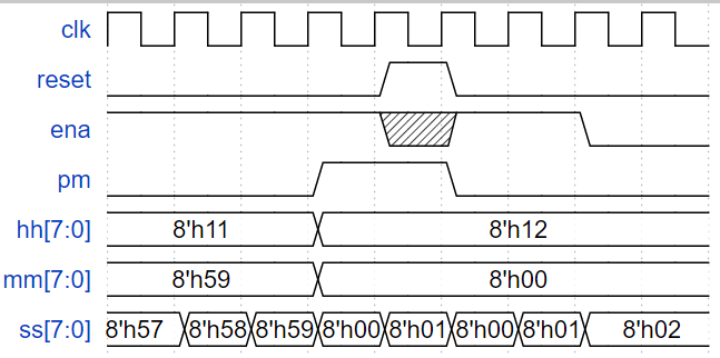
-
Code Block
module top_module(
    input clk,
    input reset,
    input ena,
    output pm,
    output [7:0] hh,
    output [7:0] mm,
    output [7:0] ss);
    reg pm_temp;
    reg [3:0] ss_ones, ss_tens;//秒的个位和十位
    reg [3:0] mm_ones, mm_tens;//分的个位和十位
    reg [3:0] hh_ones, hh_tens;//时的个位和十位

    wire	add_ss_ones, add_ss_tens, end_ss_ones, end_ss_tens;//秒的个位和十位的加法与减法的使能位
    wire	add_mm_ones, end_mm_ones, add_mm_tens, end_mm_tens;//分的个位和十位的加法与减法的使能位
    wire	add_hh_ones, end_hh_ones_0, end_hh_ones_1, add_hh_tens, end_hh_tens_0, end_hh_tens_1;时的个位和十位的加法与减法的使能位
    wire	pm_flag;//上午下午切换位

    assign add_ss_ones = ena;//使能端决定秒的个位能否开始运行
    assign end_ss_ones = add_ss_ones && (ss_ones == 4'd9);//秒的个位数运行时和秒的个位数到9后,向十位进位

    always@(posedge clk)	begin	//秒的个位数加法
        if(reset || (add_ss_ones && end_ss_ones))	begin
            ss_ones <= 4'd0;
        end
        else if (add_ss_ones)	begin
            ss_ones <= ss_ones + 4'd1;
        end
    end

    assign add_ss_tens = end_ss_ones;		//个位向十位进位,十位开始工作
    assign end_ss_tens = add_ss_tens && (ss_tens == 4'd5);	//秒的十位为5,并且秒十位工作时,秒的十位向分的个位进位
    always @(posedge clk)begin
        if(reset || (add_ss_tens && end_ss_tens))begin
            ss_tens <= 4'b0;
        end
        else if(add_ss_tens)begin
            ss_tens <= ss_tens + 4'b1;
        end
    end

    assign add_mm_ones = end_ss_tens;	//秒的十位数向分的个位数进位,分的个位数开始工作
    assign end_mm_ones = add_mm_ones && (mm_ones == 4'd9);	//分的个位数为9,并且分的个位数工作时,分的个位数向分的十位数进位
    always @(posedge clk)begin
        if(reset || (add_mm_ones && end_mm_ones))begin
            mm_ones <= 4'b0;
        end
        else if(add_mm_ones)begin
            mm_ones <= mm_ones + 4'b1;
        end
    end

    assign add_mm_tens = end_mm_ones;	//分的个位数向十位数进位,分的十位数开始工作
    assign end_mm_tens = add_mm_tens && (mm_tens == 4'd5);	//分的十位数为5,并且分十位在工作时,分的十位数向时的个位数进位
	always @(posedge clk)begin
        if(reset || (add_mm_tens && end_mm_tens))begin
            mm_tens <= 4'b0;
        end
        else if(add_mm_tens)begin
            mm_tens <= mm_tens + 4'b1;
        end
    end

    assign add_hh_ones = end_mm_tens;	//分的十位数向时的个位数进位,时的个位数开始工作
    assign end_hh_ones_0 = add_hh_ones && (hh_ones == 4'd9);	//时的个位数为9,并且时的个位数在工作时,时的十位数进位
    assign end_hh_ones_1 = add_hh_ones && ( (hh_tens == 4'd1) && (hh_ones == 4'd2));//时的十位数为1,个位数为2,上午下午转换
    always @(posedge clk)begin
        if(reset)begin
            hh_ones <= 4'd2;	//重置时为12:00AM,时的个位数为2
        end
        else if(add_hh_ones)begin
            if(end_hh_ones_0)begin
                hh_ones <= 4'b0;
            end
            else if(end_hh_ones_1)begin
                hh_ones <= 4'b1; //12点过完到01点
            end
            else begin
                hh_ones <= hh_ones+4'b1;
            end
        end
    end

    assign add_hh_tens = end_mm_tens;	//时的个位数向时的十位数进位,时的十位数工作位置1
    assign end_hh_tens_0 = add_hh_tens && end_hh_ones_0;//时十位数正常进位,并且时的十位数工作位置1,时的十位数开始工作。
    assign end_hh_tens_1 = add_hh_tens && end_hh_ones_1;//上午下午转换,并且时的十位数工作位置1,时的十位数跳为0
    always @(posedge clk)begin
        if(reset)begin
            hh_tens <= 4'b1;	//重置时为12:00AM,时的十位数为1
        end
        else if(add_hh_tens)begin
            if(end_hh_tens_1)begin
                hh_tens <= 4'b0;
            end
            else if(end_hh_tens_0)begin
                hh_tens <= hh_tens + 4'b1;
            end
        end
    end

    always@(posedge clk)begin
        if(reset)begin
            pm_temp <= 1'b0;//重置为上午
        end
        else if(pm_flag)begin
            pm_temp <= ~pm_temp;//上午下午切换
        end
    end

    assign pm_flag = hh_tens == 4'd1 && hh_ones == 4'd1 && end_mm_tens;//11点59分,上午下午转换

    assign ss = {ss_tens, ss_ones};
    assign mm = {mm_tens, mm_ones};
    assign hh = {hh_tens, hh_ones};
    assign pm = pm_temp;


endmodule
Shift Registers
4-bit shift register
-
Problem Statement
Build a 4-bit shift register (right shift), with asynchronous reset, synchronous load, and enable.
areset: Resets shift register to zero.load: Loads shift register withdata[3:0]instead of shifting.ena: Shift right (q[3]becomes zero,q[0]is shifted out and disappears).q: The contents of the shift register.
If both the
loadandenainputs are asserted (1), theloadinput has higher priority. -
Code Block
module top_module(
    input clk,
    input areset,  // async active-high reset to zero
    input load,
    input ena,
    input [3:0] data,
    output reg [3:0] q);
    always @(posedge clk or posedge areset)	begin
        if(areset)		begin
            q <= 4'd0;
        end
        else if(load)	begin	//load要在ena上面,因为load优先级更高
            q <= data;
        end
        else if(ena)	begin
            q <= {1'd0, q[3:1]}; //右移位
        end
    end
endmodule
Left/right rotator
-
Problem Statement
Build a 100-bit left/right rotator, with synchronous load and left/right enable. A rotator shifts-in the shifted-out bit from the other end of the register, unlike a shifter that discards the shifted-out bit and shifts in a zero. If enabled, a rotator rotates the bits around and does not modify/discard them.
-
load: Loads shift register withdata[99:0]instead of rotating. -
-
ena[1:0]
- Chooses whether and which direction to rotate.
2'b01rotates right by one bit2'b10rotates left by one bit2'b00and2'b11do not rotate.
-
q: The contents of the rotator.
-
-
Code Block
module top_module(
    input clk,
    input load,
    input [1:0] ena,
    input [99:0] data,
    output reg [99:0] q);
    always@(posedge clk)	begin
        if(load)	begin
            q <= data;
        end
        else	begin
            case(ena)
                2'b01 : q <= {q[0],q[99:1]};
                2'b10 : q <= {q[98:0],q[99]};
                2'b00,2'b11 : q <= q;
            endcase
        end
    end
endmodule
Left/right arithmetic shift by 1 or 8
-
Problem Statement
Build a 64-bit arithmetic shift register, with synchronous load. The shifter can shift both left and right, and by 1 or 8 bit positions, selected by
amount.An arithmetic right shift shifts in the sign bit of the number in the shift register (
q[63]in this case) instead of zero as done by a logical right shift. Another way of thinking about an arithmetic right shift is that it assumes the number being shifted is signed and preserves the sign, so that arithmetic right shift divides a signed number by a power of two.There is no difference between logical and arithmetic left shifts.
-
load: Loads shift register withdata[63:0]instead of shifting. -
ena: Chooses whether to shift. -
-
amount
- Chooses which direction and how much to shift.
2'b00: shift left by 1 bit.2'b01: shift left by 8 bits.2'b10: shift right by 1 bit.2'b11: shift right by 8 bits.
-
q: The contents of the shifter.
-
-
Code Block
module top_module(
    input clk,
    input load,
    input ena,
    input [1:0] amount,
    input [63:0] data,
    output reg [63:0] q);

    always@(posedge clk)	begin
        if(load)	begin
            q <= data;
        end
        else if(ena) begin
            case(amount)
                2'b00 : q <= {q[62:0],    1'b0};
                2'b01 : q <= {q[55:0],    8'b0};
                2'b10 : q <= {q[63],      q[63:1]};
                2'b11 : q <= {{8{q[63]}}, q[63:8]};
            endcase
        end
    end
endmodule
5-bit LFSR
-
Problem Statement
A linear feedback shift register is a shift register usually with a few XOR gates to produce the next state of the shift register. A Galois LFSR is one particular arrangement where bit positions with a “tap” are XORed with the output bit to produce its next value, while bit positions without a tap shift. If the taps positions are carefully chosen, the LFSR can be made to be “maximum-length”. A maximum-length LFSR of n bits cycles through 2n-1 states before repeating (the all-zero state is never reached).
The following diagram shows a 5-bit maximal-length Galois LFSR with taps at bit positions 5 and 3. (Tap positions are usually numbered starting from 1). Note that I drew the XOR gate at position 5 for consistency, but one of the XOR gate inputs is 0.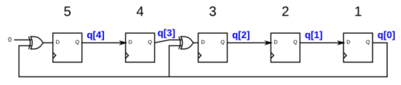
问题示意图(转自HDLBits) -
Code Block
module top_module(
    input clk,
    input reset,    // Active-high synchronous reset to 5'h1
    output [4:0] q
);
    always@(posedge clk)	begin
        if (reset)	begin
            q <= 5'd1;
        end
        else begin
            q[4] <= q[0] ^ 1'b0;	//第一个D触发器,默认输入为1'b0,下面依次类推
            q[3] <= q[4];
            q[2] <= q[0] ^ q[3];
            q[1] <= q[2];
            q[0] <= q[1];
        end
    end
endmodule
3-bit LFSR
-
Problem Statement
Write the Verilog code for this sequential circuit (Submodules are ok, but the top-level must be named
top_module). Assume that you are going to implement the circuit on the DE1-SoC board. Connect theRinputs to theSWswitches, connect Clock toKEY[0], andLtoKEY[1]. Connect theQoutputs to the red lightsLEDR.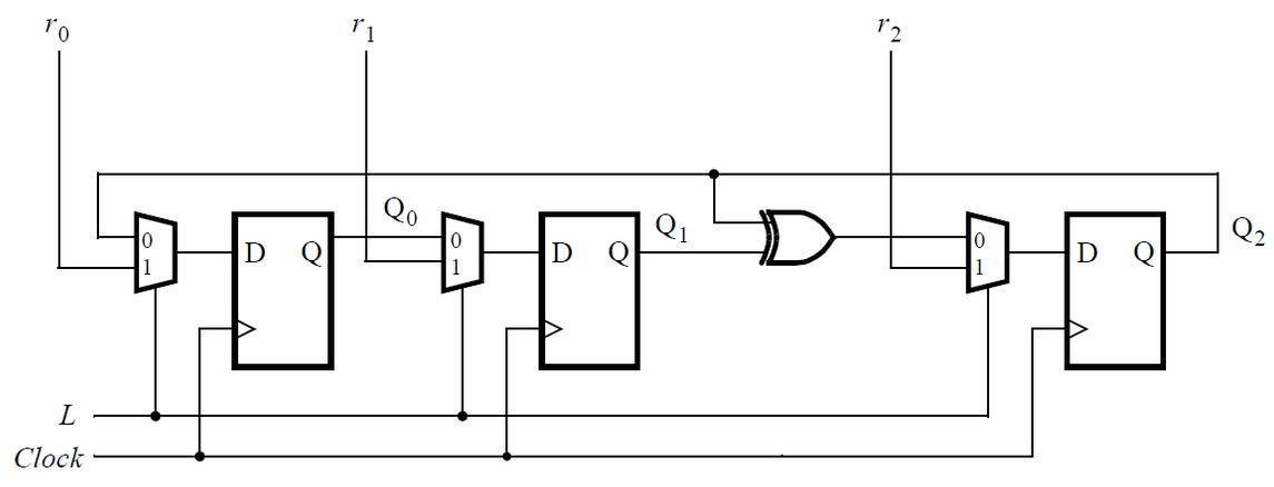
-
Code Block
module top_module (
	input [2:0] SW,      // R
	input [1:0] KEY,     // L and clk
	output [2:0] LEDR);  // Q

    always@(posedge KEY[0]) begin
        if(KEY[1])	begin
            LEDR[0] <= SW[0];
            LEDR[1] <= SW[1];
            LEDR[2] <= SW[2];
        end
        else	begin
            LEDR[0] <= LEDR[2];
            LEDR[1] <= LEDR[0];
            LEDR[2] <= LEDR[2] ^ LEDR[1];
        end
    end
endmodule
32-bit LFSR
-
Problem Statement
Build a 32-bit Galois LFSR with taps at bit positions 32, 22, 2, and 1.
-
Code Block
module top_module(
    input clk,
    input reset,    // Active-high synchronous reset to 32'h1
    output [31:0] q
);
    integer i;
    always@(posedge clk)	begin
        if(reset)	begin
            q <= 32'b1;
        end
        else	begin
            for(i=0; i<32; i++)	begin
                if(i==31)	begin
                    q[i] <= q[0] ^ 1'b0;
                end
                else if(i==21 || i==1 || i==0)	begin
                    q[i] <= q[i+1] ^ q[0];
                end
                else	begin
                    q[i] <= q[i+1];
                end
            end
        end
    end
endmodule
Shift register_1
-
Problem Statement
Implement the following circuit:
-
Code Block
module top_module (
    input clk,
    input resetn,   // synchronous reset
    input in,
    output out);
    reg [2:0] q;
    always@(posedge clk)	begin
        if(resetn == 0)	begin
            {out, q[2:0]} <= 4'b0;
        end
        else if(resetn)	begin
            {out, q[2:0]} <= {q[2:0], in};
        end
    end

endmodule
Shift register_2
-
Problem Statement
Write a top-level Verilog module (named top_module) for the shift register, assuming that n = 4. Instantiate four copies of your MUXDFF subcircuit in your top-level module. Assume that you are going to implement the circuit on the DE2 board.
- Connect the R inputs to the SW switches,
- clk to KEY[0],
- E to KEY[1],
- L to KEY[2], and
- w to KEY[3].
- Connect the outputs to the red lights LEDR[3:0].
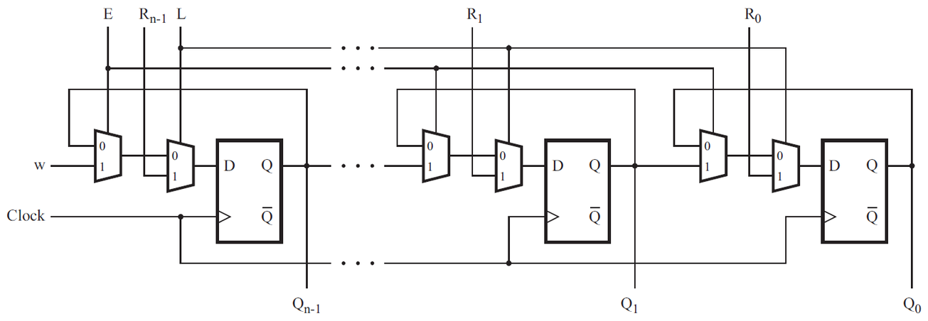
-
Code Block
module top_module (
    input [3:0] SW,
    input [3:0] KEY,
    output [3:0] LEDR
); //
    MUXDFF muxdff_0(.clk(KEY[0]), .E(KEY[1]), .L(KEY[2]), .w(LEDR[1]), .R(SW[0]), .Q(LEDR[0]) );
    MUXDFF muxdff_1(.clk(KEY[0]), .E(KEY[1]), .L(KEY[2]), .w(LEDR[2]), .R(SW[1]), .Q(LEDR[1]) );
    MUXDFF muxdff_2(.clk(KEY[0]), .E(KEY[1]), .L(KEY[2]), .w(LEDR[3]), .R(SW[2]), .Q(LEDR[2]) );
    MUXDFF muxdff_3(.clk(KEY[0]), .E(KEY[1]), .L(KEY[2]), .w(KEY[3]),  .R(SW[3]), .Q(LEDR[3]) );

endmodule

module MUXDFF (
    		   input clk,
               input w, E, L, R ,
               output Q
              );
   	wire temp_q;
    assign temp_q = E ? w : Q; //第一个2选1数据选择器
    always@(posedge clk)	begin
        if(L)	begin
            Q <= R;
        end
        else	begin
            Q <= temp_q;
        end
    end
endmodule
3-input LUT
-
Problem Statement
In this question, you will design a circuit for an 8x1 memory, where writing to the memory is accomplished by shifting-in bits, and reading is “random access”, as in a typical RAM. You will then use the circuit to realize a 3-input logic function.
First, create an 8-bit shift register with 8 D-type flip-flops. Label the flip-flop outputs from Q[0]…Q[7]. The shift register input should be called S, which feeds the input of Q[0] (MSB is shifted in first). The enable input controls whether to shift. Then, extend the circuit to have 3 additional inputs A,B,C and an output Z. The circuit’s behaviour should be as follows: when ABC is 000, Z=Q[0], when ABC is 001, Z=Q[1], and so on. Your circuit should contain ONLY the 8-bit shift register, and multiplexers. (Aside: this circuit is called a 3-input look-up-table (LUT)).
-
Code Block
module top_module (
    input clk,
    input enable,
    input S,
    input A, B, C,
    output Z );
    reg [7:0] Q;
    always@(posedge clk)	begin
        if(enable)	begin
            Q <= {Q[6:0], S};
        end
    end
    assign Z = Q[{A,B,C}];

endmodule
More Circuits
Rule 90
-
Problem Statement
The rules are simple. There is a one-dimensional array of cells (on or off). At each time step, the next state of each cell is the XOR of the cell’s two current neighbours. A more verbose way of expressing this rule is the following table, where a cell’s next state is a function of itself and its two neighbours:
In this circuit, create a 512-cell system (
q[511:0]), and advance by one time step each clock cycle. Theloadinput indicates the state of the system should be loaded withdata[511:0]. Assume the boundaries (q[-1]andq[512]) are both zero (off).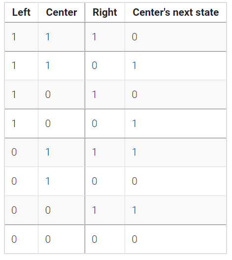
-
Code Block
module top_module(
    input clk,
    input load,
    input [511:0] data,
    output [511:0] q );
    always@(posedge clk)	begin
        if(load)	begin
            q <= data;
        end
        else	begin
            q <= {1'b0, q[511:1]} ^ {q[510:0], 1'b0};//当前位为相邻两位的异或,故为q[511:0] <= q[512:1] ^ q[511:-1]
        end
    end
endmodule
Rule 110
-
Problem Statement
There is a one-dimensional array of cells (on or off). At each time step, the state of each cell changes. In Rule 110, the next state of each cell depends only on itself and its two neighbours, according to the following table:
In this circuit, create a 512-cell system (
q[511:0]), and advance by one time step each clock cycle. Theloadinput indicates the state of the system should be loaded withdata[511:0]. Assume the boundaries (q[-1]andq[512]) are both zero (off).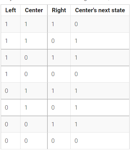
问题示意图(转自HDLBits) -
Code Block
module top_module(
    input clk,
    input load,
    input [511:0] data,
    output [511:0] q
);
    always @(posedge clk)begin
        if(load)begin
        	q <= data;
        end
        else begin
            q <= (~{1'b0, q[511:1]} & q) | (q & ~{q[510:0], 1'b0}) | {~{1'b0, q[511:1]} & {q[510:0], 1'b0}} | {~q & {q[510:0], 1'b0}};
        end
    end

endmodule
Conway’s Game of Life 16x16
-
Problem Statement
The “game” is played on a two-dimensional grid of cells, where each cell is either 1 (alive) or 0 (dead). At each time step, each cell changes state depending on how many neighbours it has:
- 0-1 neighbour: Cell becomes 0.
- 2 neighbours: Cell state does not change.
- 3 neighbours: Cell becomes 1.
- 4+ neighbours: Cell becomes 0.
The game is formulated for an infinite grid. In this circuit, we will use a 16x16 grid. To make things more interesting, we will use a 16x16 toroid, where the sides wrap around to the other side of the grid. For example, the corner cell (0,0) has 8 neighbours:
(15,1),(15,0),(15,15),(0,1),(0,15),(1,1),(1,0), and(1,15). The 16x16 grid is represented by a length 256 vector, where each row of 16 cells is represented by a sub-vector: q[15:0] is row 0, q[31:16] is row 1, etc. (This tool accepts SystemVerilog, so you may use 2D vectors if you wish.)load: Loadsdataintoqat the next clock edge, for loading initial state.q: The 16x16 current state of the game, updated every clock cycle.
The game state should advance by one timestep every clock cycle.
-
Code Block
module top_module(
    input clk,
    input load,
    input [255:0] data,
    output [255:0] q );

    reg [3:0] count;
    integer i;

    always @(posedge clk)begin
        if(load)begin
        	q <= data;
        end
        else begin
            for(i=0;i<256;i++)begin
                if(i == 0)	begin
                    count = q[255] + q[240] + q[241] + q[15] + q[1] + q[31] + q[16] + q[17];
                end
                else if(i == 15)	begin
                    count = q[254] + q[255] + q[240] + q[14] + q[0] + q[30] + q[31] + q[16];
                end
                else if(i == 240)	begin
                    count = q[239] + q[224] + q[225] + q[255] + q[241] + q[15] + q[0] + q[1];
                end
                else if(i == 255)	begin
                    count = q[238] + q[239] + q[224] + q[254] + q[240] + q[15] + q[0] + q[14];
                end
                else if( i>0 && i<15)	begin
                    count = q[239+i]+q[240+i]+q[241+i]+q[i-1]+q[i+1]+q[i+15]+q[i+16]+q[i+17];
                end
                else if(i>240 && i<255)	begin
                    count = q[i-17]+q[i-16]+q[i-15]+q[i-1]+q[i+1]+q[i-239]+q[i-240]+q[i-241];
                end
                else if( i%16 == 0)		begin
                    count = q[i-1]+q[i-16]+q[i-15]+q[i+15]+q[i+1]+q[i+31]+q[i+16]+q[i+17];
                end
                else if(i % 16 == 15)	begin
                    count = q[i-17]+q[i-16]+q[i-31]+q[i-1]+q[i-15]+q[i+15]+q[i+16]+q[i+1];
                end
                else	begin
                    count = q[i-17]+q[i-16]+q[i-15]+q[i-1]+q[i+1]+q[i+15]+q[i+16]+q[i+17];
                end

                case(count)
                    4'd2:q[i] <= q[i];
                    4'd3:q[i] <= 1'b1;
                    default:q[i] <= 1'b0;
                endcase
            end
        end
    end

endmodule
最后
以上就是感性香烟最近收集整理的关于HDLBits刷题全记录(四)的全部内容,更多相关HDLBits刷题全记录(四)内容请搜索靠谱客的其他文章。


发表评论 取消回复