DSP48E1 (primitive)原语例化实例
之前倒腾dsp48e1的时候发现网上虽然有一些文章,但是大部分都是无用的文章,
正如某位同仁说的,高手都忙于泡妞,哪有精力来写文章,
把之前倒腾的代码贴出来供大家参考。
先把OPMODE和ALUMODE贴上,来自网上的文章
OPMODE用来决定下面这个图X,Y,Z这些mux的选择,一时半会看不懂,稍微花点时间是可以看懂的
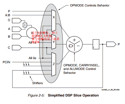
上图有两个X,圆圈里面的那个X是乘法,输出就是下面表格里的M,右边的这个X才是下面表格里的MUX X
| Z OPMODE[6:4] | Y OPMODE[3:2] | X OPMODE[1:0] | X Multiplexer Output | Notes |
| xxx | xx | 00 | 0 | Default |
| xxx | 01 | 01 | M | Must select with OPMODE[3:2] = 01 |
| xxx | xx | 10 | P | Must select with PREG = 1 |
| xxx | xx | 11 | A:B | 48 bits wide |
这个表格表示X的选择
可以选择M,P或者A:B,
01选M,10选P,11选A:B
| Z OPMODE[6:4] | Y OPMODE[3:2] | X OPMODE[1:0] | Y Multiplexer Output | Notes |
| xxx | 00 | xx | 0 | Default |
| xxx | 01 | 01 | M | Must select with OPMODE[1:0] = 01 |
| xxx | 10 | xx | 48'FFFFFFFFFFFF | Used mainly for logic unit bitwise operations on the X and Z multiplexers |
| xxx | 11 | xx | C | |
这个表格表示Y的选择,
| Z OPMODE[6:4] | Y OPMODE[3:2] | X OPMODE[1:0] | Z Multiplexer Output | Notes |
| 000 | xx | xx | 0 | Default |
| 001 | xx | xx | PCIN | |
| 010 | xx | xx | P | Must select with PREG = 1 |
| 011 | xx | xx | C | |
| 100 | 10 | 00 | P | Use for MACC extend only. Must select with PREG = 1 |
| 101 | xx | xx | 17-bit Shift (PCIN) | |
| 110 | xx | xx | 17-bit Shift (P) | Must select with PREG = 1 |
| 111 | xx | xx | xx | Illegal selection |
这个表格表示Z的选择
ALUMODE
4位ALUMODE控制第二阶段加/减/逻辑单元的行为。
ALUMODE = 0000 选择表单Z + (X + Y)的添加操作。
ALUMODE = 0011 选择Z - (X + Y )形式的减运算。
ALUMODE = 0001 可以实现- z + (X + Y) - 1 = not (Z) + X + Y。
ALUMODE = 0010 可以实现 - (Z + X + Y) - 1 = not (Z + X + Y)。
2的补数的负数是通过按位反转和加1得到的,例如-k = not (k) + 1。
INMODE暂时还没试验过
| INMODE[3] | INMODE[2] | INMODE[1] | INMODE[0] | USE_DPORT | Multiplier A Port |
| 0 | 0 | 0 | 0 | FALSE | A2 |
| 0 | 0 | 0 | 1 | FALSE | A1 |
| 0 | 0 | 1 | 0 | FALSE | Zero |
| 0 | 0 | 1 | 1 | FALSE | Zero |
| 0 | 0 | 0 | 0 | TRUE | A2 |
| 0 | 0 | 0 | 1 | TRUE | A1 |
| 0 | 0 | 1 | 0 | TRUE | Zero |
| 0 | 0 | 1 | 1 | TRUE | Zero |
| 0 | 1 | 0 | 0 | TRUE | D + A2(1) |
| 0 | 1 | 0 | 1 | TRUE | D + A1(1) |
| 0 | 1 | 1 | 0 | TRUE | D |
| 0 | 1 | 1 | 1 | TRUE | D |
| 1 | 0 | 0 | 0 | TRUE | -A2 |
| 1 | 0 | 0 | 1 | TRUE | -A1 |
| 1 | 0 | 1 | 0 | TRUE | Zero |
| 1 | 0 | 1 | 1 | TRUE | Zero |
| 1 | 1 | 0 | 0 | TRUE | D – A2(1) |
| 1 | 1 | 0 | 1 | TRUE | D – A1(1) |
| 1 | 1 | 1 | 0 | TRUE | D |
| 1 | 1 | 1 | 1 | TRUE | D |
| INMODE[4] | Multiplier B Port |
| 0 | B2 |
| 1 | B1 |
之前尝试例化dsp48e1的时候,google百度都解决不了问题,直接拿dsp48e1的代码来仿,这样还更快一点,
为了节省大家的时间,我把DSP48E1的仿真工程放到github里,大家可以下载下来调试,
https://github.com/tishi43/dsp48e1
加了如下中间变量的打印,如果结果不如预期,可以观察这些变量,继续跟踪哪步结果异常,
a_o_mux根据A_INPUT=DIRECT还是CASCADE 选择a_in,还是acin_in
qd_o_mux 根据DREG,选择d_in还是延迟一周期的d_in
ad_addsub, 顾名思义,就是选择A+D,还是A-D
直接上代码更直观一点
assign ad_addsub = qinmode_o_mux[3]?(-a_preaddsub + (qinmode_o_mux[2]?qd_o_mux:25'b0)):(a_preaddsub + (qinmode_o_mux[2]?qd_o_mux:25'b0));
qad_o_mux 根据ADREG=0还是1,选择ad_addsub还是延迟一周期的ad_addsub
mult_o就是上面图中(A+D)*B的结果,即M
qopmode_o_mux,根据OPMODEREG,选择opmode_in还是延迟1周期的opmode_in
qx_o_mux,上图中X的选择,选择M,还是A:B,还是P
alu_o差不多最终的结果了,直接看代码更容易理解
qp_o_mux,根据PREG选择alu_o还是alu_o延迟1周期
qc_o_mux,根据CREG选择c_in还是c_in延迟1周期
qz_o_mux,第三个表格中Z的选择
下面是之前我调试时的打印,把.USE_DPORT误设为TRUE时,结果为0,可以看到mult_o这一步为0了,再跟着代码拉几根信号到波形窗口,就发现问题了,
run 1us
# 0 a_o_mux[24:0] x
# 0 ADREG1 qad_o_mux 0
# 0 ALU qx_o_mux x qx_o_mux x qz_o_mux 0
# 0 qopmode_o_mux[1:0] 1 qx_o_mux x
# 0 ALU qx_o_mux x qx_o_mux 0 qz_o_mux 0
# 200000 a_o_mux[24:0] 100
# 200000 ad_addsub[24:0] 100 qinmode_o_mux[3] 0 a_preaddsub[24:0] 100 qinmode_o_mux[2] 0 qd_o_mux[24:0] 0
# 200000 a_preaddsub[24:0] 100 qinmode_o_mux[1] 0 qinmode_o_mux[0] 0 qa_o_reg1[24:0] 0 qa_o_mux[24:0] 100
# 200000 qopmode_o_mux[1:0] 1 qx_o_mux x
# 200000 mult_o 0
# 200000 qopmode_o_mux[1:0] 1 qx_o_mux x
# 200000 ALU qx_o_mux 0 qx_o_mux 0 qz_o_mux 0
# 200000 alu_o 0
# 200001 qopmode_o_mux[1:0] 1 qx_o_mux 0
# p 0
不求弄清每种组合会是什么情况,只求最常用的一些用法,如下
1 assgin o=in1*in2 立即出结果
AREG,BREG,MREG,PREG设0
CREG,DREG,ADREG实际没有用到,这些设为1其实也无意义
CLK脚可以填0,也可以填实际时钟
ALUMODE=0
OPMODE=7'b0000101
`timescale 1ns / 10ps // timescale time_unit/time_presicion
module test(
    input wire clk,
    input wire rst,
    input wire signed [24:0] in1,
    input wire signed [17:0] in2,
    output wire signed [47:0]  o,
    output wire signed [29:0] acout,
    output wire signed [17:0] bcout,
    output wire [3:0] carryout,
    output wire [3:0] carrycasout,
    output wire signed [47:0] pcout
);
DSP48E1 #(
.A_INPUT("DIRECT"),
.B_INPUT("DIRECT"),
.USE_DPORT("FALSE"),
.USE_MULT("MULTIPLY"),
.USE_SIMD("ONE48"),
.AUTORESET_PATDET("NO_RESET"),    // "NO_RESET", "RESET_MATCH", "RESET_NOT_MATCH"
.MASK(48'h3fffffffffff),          // 48-bit mask value for pattern detect (1=ignore)
.PATTERN(48'h000000000000),       // 48-bit pattern match for pattern detect
.SEL_MASK("MASK"),           // "C", "MASK", "ROUNDING_MODE1", "ROUNDING_MODE2"
.SEL_PATTERN("PATTERN"),          // Select pattern value ("PATTERN" or "C")
.USE_PATTERN_DETECT("NO_PATDET"),  // Enable pattern detect ("PATDET" or "NO_PATDET")
// Register Control Attributes: Pipeline Register Configuration
.ACASCREG(0),            //
.ADREG(1),               // Number of pipeline stages for pre-adder (0 or 1)
.ALUMODEREG(0),          // Number of pipeline stages for ALUMODE (0 or 1)
.AREG(0),                 // Number of pipeline stages for A (0, 1 or 2)
.BCASCREG(0),            // Number of pipeline stages between B/BCIN and BCOUT (0, 1 or 2)
.BREG(0),                         // Number of pipeline stages for B (0, 1 or 2)
.CARRYINREG(0),                   // Number of pipeline stages for CARRYIN (0 or 1)
.CARRYINSELREG(0),                // Number of pipeline stages for CARRYINSEL (0 or 1)
.CREG(1),                         // Number of pipeline stages for C (0 or 1)
.DREG(1),                         // Number of pipeline stages for D (0 or 1)
.INMODEREG(0),                    // Number of pipeline stages for INMODE (0 or 1)
.MREG(0),                         // Number of multiplier pipeline stages (0 or 1)
.OPMODEREG(0),                    // Number of pipeline stages for OPMODE (0 or 1)
.PREG(0)                          // Number of pipeline stages for P (0 or 1)
   )
DSP48E1_inst (
// Cascade: 30-bit (each) output: Cascade Ports
.ACOUT(acout),                   // 30-bit output: A port cascade output
.BCOUT(bcout),                   // 18-bit output: B port cascade output
.CARRYCASCOUT(carrycasout),     // 1-bit output: Cascade carry output
.MULTSIGNOUT(),       // 1-bit output: Multiplier sign cascade output
.PCOUT(pcout),                   // 48-bit output: Cascade output
//这些引脚空着就好
// Control: 1-bit (each) output: Control Inputs/Status Bits
.OVERFLOW(),             // 1-bit output: Overflow in add/acc output
.PATTERNBDETECT(),        // 1-bit output: Pattern bar detect output
.PATTERNDETECT(),   // 1-bit output: Pattern detect output
.UNDERFLOW(),           // 1-bit output: Underflow in add/acc output
//这些引脚也空着,没用
// Data: 4-bit (each) output: Data Ports
.CARRYOUT(carryout),                               // 4-bit output: Carry output
.P(o),                           // 48-bit output: Primary data output
//P输出48bit的
// Cascade: 30-bit (each) input: Cascade Ports
.ACIN(30'b0),                     // 30-bit input: A cascade data input
.BCIN(18'b0),                     // 18-bit input: B cascade input
.CARRYCASCIN(1'b0),              // 1-bit input: Cascade carry input
.MULTSIGNIN(1'b0),         // 1-bit input: Multiplier sign input
.PCIN(48'b0),                     // 48-bit input: P cascade input
//这些引脚很重要,做流水线时,数据又这几个引脚输入。
// Control: 4-bit (each) input: Control Inputs/Status Bits
.ALUMODE(4'b0),               // 4-bit input: ALU control input
.CARRYINSEL(3'b0),         // 3-bit input: Carry select input
.CLK(0),                       // 1-bit input: Clock input
.INMODE(5'b0),                 // 5-bit input: INMODE control input
.OPMODE(7'b0000101),                 // 7-bit input: Operation mode input
// Data: 30-bit (each) input: Data Ports
.A(in1),                           // 30-bit input: A data input
.B(in2),                           // 18-bit input: B data input
.C(48'hffffffffffff),              // 48-bit input: C data input
.CARRYIN(1'b0),                      // 1-bit input: Carry input signal
.D(25'b0),                           // 25-bit input: D data input
// Reset/Clock Enable: 1-bit (each) input: Reset/Clock Enable Inputs
.CEA1(1'b0),                      // 1-bit input: Clock enable input for 1st stage AREG
.CEA2(1'b0),                      // 1-bit input: Clock enable input for 2nd stage AREG
.CEAD(1'b0),                      // 1-bit input: Clock enable input for ADREG
.CEALUMODE(1'b0),                 // 1-bit input: Clock enable input for ALUMODE
.CEB1(1'b0),                      // 1-bit input: Clock enable input for 1st stage BREG
.CEB2(1'b0),                      // 1-bit input: Clock enable input for 2nd stage BREG
.CEC(1'b0),                       // 1-bit input: Clock enable input for CREG
.CECARRYIN(1'b0),                 // 1-bit input: Clock enable input for CARRYINREG
.CECTRL(1'b0),                    // 1-bit input: Clock enable input for OPMODEREG and CARRYINSELREG
.CED(1'b0),                       // 1-bit input: Clock enable input for DREG
.CEINMODE(1'b0),                  // 1-bit input: Clock enable input for INMODEREG
.CEM(1'b0),                       // 1-bit input: Clock enable input for MREG
.CEP(1'b0),                       // 1-bit input: Clock enable input for PREG
.RSTA(1'b0),                       // 1-bit input: Reset input for AREG
.RSTALLCARRYIN(1'b0),              // 1-bit input: Reset input for CARRYINREG
.RSTALUMODE(1'b0),                 // 1-bit input: Reset input for ALUMODEREG
.RSTB(1'b0),                       // 1-bit input: Reset input for BREG
.RSTC(1'b0),                       // 1-bit input: Reset input for CREG
.RSTCTRL(1'b0),                    // 1-bit input: Reset input for OPMODEREG and CARRYINSELREG
.RSTD(1'b0),                       // 1-bit input: Reset input for DREG and ADREG
.RSTINMODE(1'b0),                  // 1-bit input: Reset input for INMODEREG
.RSTM(1'b0),                       // 1-bit input: Reset input for MREG
.RSTP(1'b0)                        // 1-bit input: Reset input for PREG
);
endmodule
module bitstream_tb;
reg rst;
reg dec_clk;
reg signed [24:0] a;
reg signed [17:0] b;
reg signed [47:0] d;
reg signed [47:0] c;
wire signed [47:0] p;
wire signed [29:0] ac;
wire signed [17:0] bc;
wire [3:0] co;
wire [3:0] ccas;
wire signed [47:0] pc;
initial begin
    rst = 0;
    #200 a = 100;
    #0 b = 200;
    #0 d = 45;
    #0 c = 400;
    #50 rst = 1;
    #1 rst = 0;
    #100 $display("p %d",p);
end
always
begin
    #1 dec_clk = 0;
    #1 dec_clk = 1;
end
test test_inst(
.clk(dec_clk),
.rst(rst),
.in1(a),
.in2(b),
.o(p),
.acout(ac),
.bcout(bc),
.carryout(co),
.carrycasout(ccas),
.pcout(pc)
);
endmodule
2 o <=in1*in2 延迟1周期出结果
和上面的唯一区别仅仅是是MREG=1,CEM=1,
注意CEM一定要等于1,否则结果是0
同样如果AREG=1, CEA要等于1,clock enable一定要相应置起来
延迟周期,也可以选择AREG,PREG这些,或者这些的组合,延迟多周期
`timescale 1ns / 10ps // timescale time_unit/time_presicion
module test(
    input wire clk,
    input wire rst,
    input wire signed [24:0] in1,
    input wire signed [17:0] in2,
    output wire signed [47:0]  o,
    output wire signed [29:0] acout,
    output wire signed [17:0] bcout,
    output wire [3:0] carryout,
    output wire [3:0] carrycasout,
    output wire signed [47:0] pcout
);
DSP48E1 #(
.A_INPUT("DIRECT"),
.B_INPUT("DIRECT"),
.USE_DPORT("FALSE"),
.USE_MULT("MULTIPLY"),
.USE_SIMD("ONE48"),
.AUTORESET_PATDET("NO_RESET"),    // "NO_RESET", "RESET_MATCH", "RESET_NOT_MATCH"
.MASK(48'h3fffffffffff),          // 48-bit mask value for pattern detect (1=ignore)
.PATTERN(48'h000000000000),       // 48-bit pattern match for pattern detect
.SEL_MASK("MASK"),           // "C", "MASK", "ROUNDING_MODE1", "ROUNDING_MODE2"
.SEL_PATTERN("PATTERN"),          // Select pattern value ("PATTERN" or "C")
.USE_PATTERN_DETECT("NO_PATDET"),  // Enable pattern detect ("PATDET" or "NO_PATDET")
// Register Control Attributes: Pipeline Register Configuration
.ACASCREG(0),            //
.ADREG(1),               // Number of pipeline stages for pre-adder (0 or 1)
.ALUMODEREG(0),          // Number of pipeline stages for ALUMODE (0 or 1)
.AREG(0),                 // Number of pipeline stages for A (0, 1 or 2)
.BCASCREG(0),            // Number of pipeline stages between B/BCIN and BCOUT (0, 1 or 2)
.BREG(0),                         // Number of pipeline stages for B (0, 1 or 2)
.CARRYINREG(0),                   // Number of pipeline stages for CARRYIN (0 or 1)
.CARRYINSELREG(0),                // Number of pipeline stages for CARRYINSEL (0 or 1)
.CREG(1),                         // Number of pipeline stages for C (0 or 1)
.DREG(1),                         // Number of pipeline stages for D (0 or 1)
.INMODEREG(0),                    // Number of pipeline stages for INMODE (0 or 1)
.MREG(1),                         // Number of multiplier pipeline stages (0 or 1)
.OPMODEREG(0),                    // Number of pipeline stages for OPMODE (0 or 1)
.PREG(0)                          // Number of pipeline stages for P (0 or 1)
   )
DSP48E1_inst (
// Cascade: 30-bit (each) output: Cascade Ports
.ACOUT(acout),                   // 30-bit output: A port cascade output
.BCOUT(bcout),                   // 18-bit output: B port cascade output
.CARRYCASCOUT(carrycasout),     // 1-bit output: Cascade carry output
.MULTSIGNOUT(),       // 1-bit output: Multiplier sign cascade output
.PCOUT(pcout),                   // 48-bit output: Cascade output
//这些引脚空着就好
// Control: 1-bit (each) output: Control Inputs/Status Bits
.OVERFLOW(),             // 1-bit output: Overflow in add/acc output
.PATTERNBDETECT(),        // 1-bit output: Pattern bar detect output
.PATTERNDETECT(),   // 1-bit output: Pattern detect output
.UNDERFLOW(),           // 1-bit output: Underflow in add/acc output
//这些引脚也空着,没用
// Data: 4-bit (each) output: Data Ports
.CARRYOUT(carryout),                               // 4-bit output: Carry output
.P(o),                           // 48-bit output: Primary data output
//P输出48bit的
// Cascade: 30-bit (each) input: Cascade Ports
.ACIN(30'b0),                     // 30-bit input: A cascade data input
.BCIN(18'b0),                     // 18-bit input: B cascade input
.CARRYCASCIN(1'b0),              // 1-bit input: Cascade carry input
.MULTSIGNIN(1'b0),         // 1-bit input: Multiplier sign input
.PCIN(48'b0),                     // 48-bit input: P cascade input
//这些引脚很重要,做流水线时,数据又这几个引脚输入。
// Control: 4-bit (each) input: Control Inputs/Status Bits
.ALUMODE(4'b0),               // 4-bit input: ALU control input
.CARRYINSEL(3'b0),         // 3-bit input: Carry select input
.CLK(clk),                       // 1-bit input: Clock input
.INMODE(5'b0),                 // 5-bit input: INMODE control input
.OPMODE(7'b0000101),                 // 7-bit input: Operation mode input
// Data: 30-bit (each) input: Data Ports
.A(in1),                           // 30-bit input: A data input
.B(in2),                           // 18-bit input: B data input
.C(48'hffffffffffff),              // 48-bit input: C data input
.CARRYIN(1'b0),                      // 1-bit input: Carry input signal
.D(25'b0),                           // 25-bit input: D data input
// Reset/Clock Enable: 1-bit (each) input: Reset/Clock Enable Inputs
.CEA1(1'b0),                      // 1-bit input: Clock enable input for 1st stage AREG
.CEA2(1'b0),                      // 1-bit input: Clock enable input for 2nd stage AREG
.CEAD(1'b0),                      // 1-bit input: Clock enable input for ADREG
.CEALUMODE(1'b0),                 // 1-bit input: Clock enable input for ALUMODE
.CEB1(1'b0),                      // 1-bit input: Clock enable input for 1st stage BREG
.CEB2(1'b0),                      // 1-bit input: Clock enable input for 2nd stage BREG
.CEC(1'b0),                       // 1-bit input: Clock enable input for CREG
.CECARRYIN(1'b0),                 // 1-bit input: Clock enable input for CARRYINREG
.CECTRL(1'b0),                    // 1-bit input: Clock enable input for OPMODEREG and CARRYINSELREG
.CED(1'b0),                       // 1-bit input: Clock enable input for DREG
.CEINMODE(1'b0),                  // 1-bit input: Clock enable input for INMODEREG
.CEM(1'b1),                       // 1-bit input: Clock enable input for MREG
.CEP(1'b0),                       // 1-bit input: Clock enable input for PREG
.RSTA(1'b0),                       // 1-bit input: Reset input for AREG
.RSTALLCARRYIN(1'b0),              // 1-bit input: Reset input for CARRYINREG
.RSTALUMODE(1'b0),                 // 1-bit input: Reset input for ALUMODEREG
.RSTB(1'b0),                       // 1-bit input: Reset input for BREG
.RSTC(1'b0),                       // 1-bit input: Reset input for CREG
.RSTCTRL(1'b0),                    // 1-bit input: Reset input for OPMODEREG and CARRYINSELREG
.RSTD(1'b0),                       // 1-bit input: Reset input for DREG and ADREG
.RSTINMODE(1'b0),                  // 1-bit input: Reset input for INMODEREG
.RSTM(1'b0),                       // 1-bit input: Reset input for MREG
.RSTP(1'b0)                        // 1-bit input: Reset input for PREG
);
endmodule
module bitstream_tb;
reg rst;
reg dec_clk;
reg signed [24:0] a;
reg signed [17:0] b;
reg signed [47:0] d;
reg signed [47:0] c;
wire signed [47:0] p;
wire signed [29:0] ac;
wire signed [17:0] bc;
wire [3:0] co;
wire [3:0] ccas;
wire signed [47:0] pc;
initial begin
    rst = 0;
    #200 a = 100;
    #0 b = 200;
    #0 d = 45;
    #0 c = 400;
    #50 rst = 1;
    #1 rst = 0;
    #100 $display("p %d",p);
end
always
begin
    #1 dec_clk = 0;
    #1 dec_clk = 1;
end
test test_inst(
.clk(dec_clk),
.rst(rst),
.in1(a),
.in2(b),
.o(p),
.acout(ac),
.bcout(bc),
.carryout(co),
.carrycasout(ccas),
.pcout(pc)
);
endmodule
3 o <= in1*in2+c
OPMODE=7'b0110101
`timescale 1ns / 10ps // timescale time_unit/time_presicion
module test(
    input wire clk,
    input wire rst,
    input wire signed [24:0] in1,
    input wire signed [17:0] in2,
    input wire signed [47:0] c,
    output wire signed [47:0]  o,
    output wire signed [29:0] acout,
    output wire signed [17:0] bcout,
    output wire [3:0] carryout,
    output wire [3:0] carrycasout,
    output wire signed [47:0] pcout
);
DSP48E1 #(
.A_INPUT("DIRECT"),
.B_INPUT("DIRECT"),
.USE_DPORT("FALSE"),
.USE_MULT("MULTIPLY"),
.USE_SIMD("ONE48"),
.AUTORESET_PATDET("NO_RESET"),    // "NO_RESET", "RESET_MATCH", "RESET_NOT_MATCH"
.MASK(48'h3fffffffffff),          // 48-bit mask value for pattern detect (1=ignore)
.PATTERN(48'h000000000000),       // 48-bit pattern match for pattern detect
.SEL_MASK("MASK"),           // "C", "MASK", "ROUNDING_MODE1", "ROUNDING_MODE2"
.SEL_PATTERN("PATTERN"),          // Select pattern value ("PATTERN" or "C")
.USE_PATTERN_DETECT("NO_PATDET"),  // Enable pattern detect ("PATDET" or "NO_PATDET")
// Register Control Attributes: Pipeline Register Configuration
.ACASCREG(0),            //
.ADREG(1),               // Number of pipeline stages for pre-adder (0 or 1)
.ALUMODEREG(0),          // Number of pipeline stages for ALUMODE (0 or 1)
.AREG(0),                 // Number of pipeline stages for A (0, 1 or 2)
.BCASCREG(0),            // Number of pipeline stages between B/BCIN and BCOUT (0, 1 or 2)
.BREG(0),                         // Number of pipeline stages for B (0, 1 or 2)
.CARRYINREG(0),                   // Number of pipeline stages for CARRYIN (0 or 1)
.CARRYINSELREG(0),                // Number of pipeline stages for CARRYINSEL (0 or 1)
.CREG(0),                         // Number of pipeline stages for C (0 or 1)
.DREG(0),                         // Number of pipeline stages for D (0 or 1)
.INMODEREG(1),                    // Number of pipeline stages for INMODE (0 or 1)
.MREG(0),                         // Number of multiplier pipeline stages (0 or 1)
.OPMODEREG(0),                    // Number of pipeline stages for OPMODE (0 or 1)
.PREG(1)                          // Number of pipeline stages for P (0 or 1)
   )
DSP48E1_inst (
// Cascade: 30-bit (each) output: Cascade Ports
.ACOUT(acout),                   // 30-bit output: A port cascade output
.BCOUT(bcout),                   // 18-bit output: B port cascade output
.CARRYCASCOUT(carrycasout),     // 1-bit output: Cascade carry output
.MULTSIGNOUT(),       // 1-bit output: Multiplier sign cascade output
.PCOUT(pcout),                   // 48-bit output: Cascade output
//这些引脚空着就好
// Control: 1-bit (each) output: Control Inputs/Status Bits
.OVERFLOW(),             // 1-bit output: Overflow in add/acc output
.PATTERNBDETECT(),        // 1-bit output: Pattern bar detect output
.PATTERNDETECT(),   // 1-bit output: Pattern detect output
.UNDERFLOW(),           // 1-bit output: Underflow in add/acc output
//这些引脚也空着,没用
// Data: 4-bit (each) output: Data Ports
.CARRYOUT(carryout),                               // 4-bit output: Carry output
.P(o),                           // 48-bit output: Primary data output
//P输出48bit的
// Cascade: 30-bit (each) input: Cascade Ports
.ACIN(30'b0),                     // 30-bit input: A cascade data input
.BCIN(18'b0),                     // 18-bit input: B cascade input
.CARRYCASCIN(1'b0),              // 1-bit input: Cascade carry input
.MULTSIGNIN(1'b0),         // 1-bit input: Multiplier sign input
.PCIN(48'b0),                     // 48-bit input: P cascade input
//这些引脚很重要,做流水线时,数据又这几个引脚输入。
// Control: 4-bit (each) input: Control Inputs/Status Bits
.ALUMODE(4'b0),               // 4-bit input: ALU control input
.CARRYINSEL(3'b0),         // 3-bit input: Carry select input
.CLK(clk),                       // 1-bit input: Clock input
.INMODE(5'b0),                 // 5-bit input: INMODE control input
.OPMODE(7'b0110101),                 // 7-bit input: Operation mode input
// Data: 30-bit (each) input: Data Ports
.A(in1),                           // 30-bit input: A data input
.B(in2),                           // 18-bit input: B data input
//.C(48'hffffffffffff),              // 48-bit input: C data input
.C(c),              // 48-bit input: C data input
.CARRYIN(1'b0),                      // 1-bit input: Carry input signal
.D(25'b0),                           // 25-bit input: D data input
// Reset/Clock Enable: 1-bit (each) input: Reset/Clock Enable Inputs
.CEA1(1'b0),                      // 1-bit input: Clock enable input for 1st stage AREG
.CEA2(1'b0),                      // 1-bit input: Clock enable input for 2nd stage AREG
.CEAD(1'b0),                      // 1-bit input: Clock enable input for ADREG
.CEALUMODE(1'b0),                 // 1-bit input: Clock enable input for ALUMODE
.CEB1(1'b0),                      // 1-bit input: Clock enable input for 1st stage BREG
.CEB2(1'b0),                      // 1-bit input: Clock enable input for 2nd stage BREG
.CEC(1'b0),                       // 1-bit input: Clock enable input for CREG
.CECARRYIN(1'b0),                 // 1-bit input: Clock enable input for CARRYINREG
.CECTRL(1'b0),                    // 1-bit input: Clock enable input for OPMODEREG and CARRYINSELREG
.CED(1'b0),                       // 1-bit input: Clock enable input for DREG
.CEINMODE(1'b0),                  // 1-bit input: Clock enable input for INMODEREG
.CEM(1'b0),                       // 1-bit input: Clock enable input for MREG
.CEP(1'b1),                       // 1-bit input: Clock enable input for PREG
.RSTA(rst),
.RSTALLCARRYIN(rst),
.RSTALUMODE(rst),
.RSTB(rst),
.RSTC(rst),
.RSTCTRL(rst),
.RSTD(rst),
.RSTINMODE(rst),
.RSTM(rst),
.RSTP(rst)
);
endmodule
module bitstream_tb;
reg rst;
reg dec_clk;
reg signed [24:0] a;
reg signed [17:0] b;
reg signed [47:0] d;
reg signed [47:0] c;
wire signed [47:0] p;
wire signed [29:0] ac;
wire signed [17:0] bc;
wire [3:0] co;
wire [3:0] ccas;
wire signed [47:0] pc;
initial begin
    rst = 0;
    #200 a = 100;
    #0 b = 200;
    #0 d = 45;
    #0 c = 400;
    #50 rst = 1;
    #1 rst = 0;
    #100 $display("p %d",p);
end
always
begin
    #1 dec_clk = 0;
    #1 dec_clk = 1;
end
test test_inst(
.clk(dec_clk),
.rst(rst),
.in1(a),
.in2(b),
.c(c),
.o(p),
.acout(ac),
.bcout(bc),
.carryout(co),
.carrycasout(ccas),
.pcout(pc)
);
endmodule
4 o <= c-in1*in2
和o <= in1*in2+c的区别是ALUMODE选0011
`timescale 1ns / 10ps // timescale time_unit/time_presicion
module test(
    input wire clk,
    input wire rst,
    input wire signed [24:0] in1,
    input wire signed [17:0] in2,
    input wire signed [47:0] c,
    output wire signed [47:0]  o,
    output wire signed [29:0] acout,
    output wire signed [17:0] bcout,
    output wire [3:0] carryout,
    output wire [3:0] carrycasout,
    output wire signed [47:0] pcout
);
DSP48E1 #(
.A_INPUT("DIRECT"),
.B_INPUT("DIRECT"),
.USE_DPORT("FALSE"),
.USE_MULT("MULTIPLY"),
.USE_SIMD("ONE48"),
.AUTORESET_PATDET("NO_RESET"),    // "NO_RESET", "RESET_MATCH", "RESET_NOT_MATCH"
.MASK(48'h3fffffffffff),          // 48-bit mask value for pattern detect (1=ignore)
.PATTERN(48'h000000000000),       // 48-bit pattern match for pattern detect
.SEL_MASK("MASK"),           // "C", "MASK", "ROUNDING_MODE1", "ROUNDING_MODE2"
.SEL_PATTERN("PATTERN"),          // Select pattern value ("PATTERN" or "C")
.USE_PATTERN_DETECT("NO_PATDET"),  // Enable pattern detect ("PATDET" or "NO_PATDET")
// Register Control Attributes: Pipeline Register Configuration
.ACASCREG(0),            //
.ADREG(1),               // Number of pipeline stages for pre-adder (0 or 1)
.ALUMODEREG(0),          // Number of pipeline stages for ALUMODE (0 or 1)
.AREG(0),                 // Number of pipeline stages for A (0, 1 or 2)
.BCASCREG(0),            // Number of pipeline stages between B/BCIN and BCOUT (0, 1 or 2)
.BREG(0),                         // Number of pipeline stages for B (0, 1 or 2)
.CARRYINREG(0),                   // Number of pipeline stages for CARRYIN (0 or 1)
.CARRYINSELREG(0),                // Number of pipeline stages for CARRYINSEL (0 or 1)
.CREG(0),                         // Number of pipeline stages for C (0 or 1)
.DREG(0),                         // Number of pipeline stages for D (0 or 1)
.INMODEREG(1),                    // Number of pipeline stages for INMODE (0 or 1)
.MREG(0),                         // Number of multiplier pipeline stages (0 or 1)
.OPMODEREG(0),                    // Number of pipeline stages for OPMODE (0 or 1)
.PREG(1)                          // Number of pipeline stages for P (0 or 1)
   )
DSP48E1_inst (
// Cascade: 30-bit (each) output: Cascade Ports
.ACOUT(acout),                   // 30-bit output: A port cascade output
.BCOUT(bcout),                   // 18-bit output: B port cascade output
.CARRYCASCOUT(carrycasout),     // 1-bit output: Cascade carry output
.MULTSIGNOUT(),       // 1-bit output: Multiplier sign cascade output
.PCOUT(pcout),                   // 48-bit output: Cascade output
//这些引脚空着就好
// Control: 1-bit (each) output: Control Inputs/Status Bits
.OVERFLOW(),             // 1-bit output: Overflow in add/acc output
.PATTERNBDETECT(),        // 1-bit output: Pattern bar detect output
.PATTERNDETECT(),   // 1-bit output: Pattern detect output
.UNDERFLOW(),           // 1-bit output: Underflow in add/acc output
//这些引脚也空着,没用
// Data: 4-bit (each) output: Data Ports
.CARRYOUT(carryout),                               // 4-bit output: Carry output
.P(o),                           // 48-bit output: Primary data output
//P输出48bit的
// Cascade: 30-bit (each) input: Cascade Ports
.ACIN(30'b0),                     // 30-bit input: A cascade data input
.BCIN(18'b0),                     // 18-bit input: B cascade input
.CARRYCASCIN(1'b0),              // 1-bit input: Cascade carry input
.MULTSIGNIN(1'b0),         // 1-bit input: Multiplier sign input
.PCIN(48'b0),                     // 48-bit input: P cascade input
//这些引脚很重要,做流水线时,数据又这几个引脚输入。
// Control: 4-bit (each) input: Control Inputs/Status Bits
.ALUMODE(4'b0011),               // 4-bit input: ALU control input
.CARRYINSEL(3'b0),         // 3-bit input: Carry select input
.CLK(clk),                       // 1-bit input: Clock input
.INMODE(5'b0),                 // 5-bit input: INMODE control input
.OPMODE(7'b0110101),                 // 7-bit input: Operation mode input
// Data: 30-bit (each) input: Data Ports
.A(in1),                           // 30-bit input: A data input
.B(in2),                           // 18-bit input: B data input
//.C(48'hffffffffffff),              // 48-bit input: C data input
.C(c),              // 48-bit input: C data input
.CARRYIN(1'b0),                      // 1-bit input: Carry input signal
.D(25'b0),                           // 25-bit input: D data input
// Reset/Clock Enable: 1-bit (each) input: Reset/Clock Enable Inputs
.CEA1(1'b0),                      // 1-bit input: Clock enable input for 1st stage AREG
.CEA2(1'b0),                      // 1-bit input: Clock enable input for 2nd stage AREG
.CEAD(1'b0),                      // 1-bit input: Clock enable input for ADREG
.CEALUMODE(1'b0),                 // 1-bit input: Clock enable input for ALUMODE
.CEB1(1'b0),                      // 1-bit input: Clock enable input for 1st stage BREG
.CEB2(1'b0),                      // 1-bit input: Clock enable input for 2nd stage BREG
.CEC(1'b0),                       // 1-bit input: Clock enable input for CREG
.CECARRYIN(1'b0),                 // 1-bit input: Clock enable input for CARRYINREG
.CECTRL(1'b0),                    // 1-bit input: Clock enable input for OPMODEREG and CARRYINSELREG
.CED(1'b0),                       // 1-bit input: Clock enable input for DREG
.CEINMODE(1'b0),                  // 1-bit input: Clock enable input for INMODEREG
.CEM(1'b0),                       // 1-bit input: Clock enable input for MREG
.CEP(1'b1),                       // 1-bit input: Clock enable input for PREG
.RSTA(rst),
.RSTALLCARRYIN(rst),
.RSTALUMODE(rst),
.RSTB(rst),
.RSTC(rst),
.RSTCTRL(rst),
.RSTD(rst),
.RSTINMODE(rst),
.RSTM(rst),
.RSTP(rst)
);
endmodule
module bitstream_tb;
reg rst;
reg dec_clk;
reg signed [24:0] a;
reg signed [17:0] b;
reg signed [47:0] d;
reg signed [47:0] c;
wire signed [47:0] p;
wire signed [29:0] ac;
wire signed [17:0] bc;
wire [3:0] co;
wire [3:0] ccas;
wire signed [47:0] pc;
initial begin
    rst = 0;
    #200 a = 10;
    #0 b = 20;
    #0 d = 45;
    #0 c = 400;
    #50 rst = 1;
    #1 rst = 0;
    #100 $display("p %d",p);
end
always
begin
    #1 dec_clk = 0;
    #1 dec_clk = 1;
end
test test_inst(
.clk(dec_clk),
.rst(rst),
.in1(a),
.in2(b),
.c(c),
.o(p),
.acout(ac),
.bcout(bc),
.carryout(co),
.carrycasout(ccas),
.pcout(pc)
);
endmodule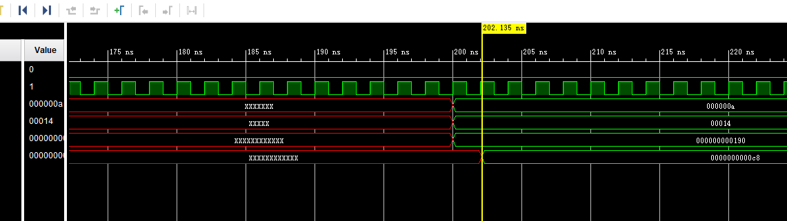
5 o <= o+in1*in2 累加操作
OPMODE=7'b0100101
`timescale 1ns / 10ps // timescale time_unit/time_presicion
module test(
    input wire clk,
    input wire rst,
    input wire signed [24:0] in1,
    input wire signed [17:0] in2,
    input wire signed [47:0] c,
    output wire signed [47:0]  o,
    output wire signed [29:0] acout,
    output wire signed [17:0] bcout,
    output wire [3:0] carryout,
    output wire [3:0] carrycasout,
    output wire signed [47:0] pcout
);
DSP48E1 #(
.A_INPUT("DIRECT"),
.B_INPUT("DIRECT"),
.USE_DPORT("FALSE"),
.USE_MULT("MULTIPLY"),
.USE_SIMD("ONE48"),
.AUTORESET_PATDET("NO_RESET"),    // "NO_RESET", "RESET_MATCH", "RESET_NOT_MATCH"
.MASK(48'h3fffffffffff),          // 48-bit mask value for pattern detect (1=ignore)
.PATTERN(48'h000000000000),       // 48-bit pattern match for pattern detect
.SEL_MASK("MASK"),           // "C", "MASK", "ROUNDING_MODE1", "ROUNDING_MODE2"
.SEL_PATTERN("PATTERN"),          // Select pattern value ("PATTERN" or "C")
.USE_PATTERN_DETECT("NO_PATDET"),  // Enable pattern detect ("PATDET" or "NO_PATDET")
// Register Control Attributes: Pipeline Register Configuration
.ACASCREG(0),            //
.ADREG(1),               // Number of pipeline stages for pre-adder (0 or 1)
.ALUMODEREG(0),          // Number of pipeline stages for ALUMODE (0 or 1)
.AREG(0),                 // Number of pipeline stages for A (0, 1 or 2)
.BCASCREG(0),            // Number of pipeline stages between B/BCIN and BCOUT (0, 1 or 2)
.BREG(0),                         // Number of pipeline stages for B (0, 1 or 2)
.CARRYINREG(0),                   // Number of pipeline stages for CARRYIN (0 or 1)
.CARRYINSELREG(0),                // Number of pipeline stages for CARRYINSEL (0 or 1)
.CREG(0),                         // Number of pipeline stages for C (0 or 1)
.DREG(0),                         // Number of pipeline stages for D (0 or 1)
.INMODEREG(1),                    // Number of pipeline stages for INMODE (0 or 1)
.MREG(0),                         // Number of multiplier pipeline stages (0 or 1)
.OPMODEREG(0),                    // Number of pipeline stages for OPMODE (0 or 1)
.PREG(1)                          // Number of pipeline stages for P (0 or 1)
   )
DSP48E1_inst (
// Cascade: 30-bit (each) output: Cascade Ports
.ACOUT(acout),                   // 30-bit output: A port cascade output
.BCOUT(bcout),                   // 18-bit output: B port cascade output
.CARRYCASCOUT(carrycasout),     // 1-bit output: Cascade carry output
.MULTSIGNOUT(),       // 1-bit output: Multiplier sign cascade output
.PCOUT(pcout),                   // 48-bit output: Cascade output
//这些引脚空着就好
// Control: 1-bit (each) output: Control Inputs/Status Bits
.OVERFLOW(),             // 1-bit output: Overflow in add/acc output
.PATTERNBDETECT(),        // 1-bit output: Pattern bar detect output
.PATTERNDETECT(),   // 1-bit output: Pattern detect output
.UNDERFLOW(),           // 1-bit output: Underflow in add/acc output
//这些引脚也空着,没用
// Data: 4-bit (each) output: Data Ports
.CARRYOUT(carryout),                               // 4-bit output: Carry output
.P(o),                           // 48-bit output: Primary data output
//P输出48bit的
// Cascade: 30-bit (each) input: Cascade Ports
.ACIN(30'b0),                     // 30-bit input: A cascade data input
.BCIN(18'b0),                     // 18-bit input: B cascade input
.CARRYCASCIN(1'b0),              // 1-bit input: Cascade carry input
.MULTSIGNIN(1'b0),         // 1-bit input: Multiplier sign input
.PCIN(48'b0),                     // 48-bit input: P cascade input
//这些引脚很重要,做流水线时,数据又这几个引脚输入。
// Control: 4-bit (each) input: Control Inputs/Status Bits
.ALUMODE(4'b0),               // 4-bit input: ALU control input
.CARRYINSEL(3'b0),         // 3-bit input: Carry select input
.CLK(clk),                       // 1-bit input: Clock input
.INMODE(5'b0),                 // 5-bit input: INMODE control input
.OPMODE(7'b0100101),                 // 7-bit input: Operation mode input
// Data: 30-bit (each) input: Data Ports
.A(in1),                           // 30-bit input: A data input
.B(in2),                           // 18-bit input: B data input
//.C(48'hffffffffffff),              // 48-bit input: C data input
.C(c),              // 48-bit input: C data input
.CARRYIN(1'b0),                      // 1-bit input: Carry input signal
.D(25'b0),                           // 25-bit input: D data input
// Reset/Clock Enable: 1-bit (each) input: Reset/Clock Enable Inputs
.CEA1(1'b0),                      // 1-bit input: Clock enable input for 1st stage AREG
.CEA2(1'b0),                      // 1-bit input: Clock enable input for 2nd stage AREG
.CEAD(1'b0),                      // 1-bit input: Clock enable input for ADREG
.CEALUMODE(1'b0),                 // 1-bit input: Clock enable input for ALUMODE
.CEB1(1'b0),                      // 1-bit input: Clock enable input for 1st stage BREG
.CEB2(1'b0),                      // 1-bit input: Clock enable input for 2nd stage BREG
.CEC(1'b0),                       // 1-bit input: Clock enable input for CREG
.CECARRYIN(1'b0),                 // 1-bit input: Clock enable input for CARRYINREG
.CECTRL(1'b0),                    // 1-bit input: Clock enable input for OPMODEREG and CARRYINSELREG
.CED(1'b0),                       // 1-bit input: Clock enable input for DREG
.CEINMODE(1'b0),                  // 1-bit input: Clock enable input for INMODEREG
.CEM(1'b0),                       // 1-bit input: Clock enable input for MREG
.CEP(1'b1),                       // 1-bit input: Clock enable input for PREG
.RSTA(rst),
.RSTALLCARRYIN(rst),
.RSTALUMODE(rst),
.RSTB(rst),
.RSTC(rst),
.RSTCTRL(rst),
.RSTD(rst),
.RSTINMODE(rst),
.RSTM(rst),
.RSTP(rst)
);
endmodule
module bitstream_tb;
reg rst;
reg dec_clk;
reg signed [24:0] a;
reg signed [17:0] b;
reg signed [47:0] d;
reg signed [47:0] c;
wire signed [47:0] p;
wire signed [29:0] ac;
wire signed [17:0] bc;
wire [3:0] co;
wire [3:0] ccas;
wire signed [47:0] pc;
initial begin
    rst = 0;
    #200 a = 100;
    #0 b = 200;
    #0 d = 45;
    #0 c = 400;
    #50 rst = 1;
    #1 rst = 0;
    #100 $display("p %d",p);
end
always
begin
    #1 dec_clk = 0;
    #1 dec_clk = 1;
end
test test_inst(
.clk(dec_clk),
.rst(rst),
.in1(a),
.in2(b),
.c(c),
.o(p),
.acout(ac),
.bcout(bc),
.carryout(co),
.carrycasout(ccas),
.pcout(pc)
);
endmodule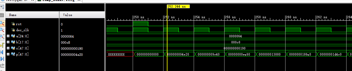
最后
以上就是幸福小土豆最近收集整理的关于DSP48E1 (primitive)原语例化实例的全部内容,更多相关DSP48E1内容请搜索靠谱客的其他文章。


发表评论 取消回复