参考文章:Verilog中的奇偶校验
在用Verilog写UART通信的逻辑代码时,遇到了"对数据做奇偶校验"的需求,网上一搜就得到了解决办法。感谢万能的网友之余,我还是想把Verilog中奇偶校验的原理用更加易于理解的方式描述一遍,故发此文。
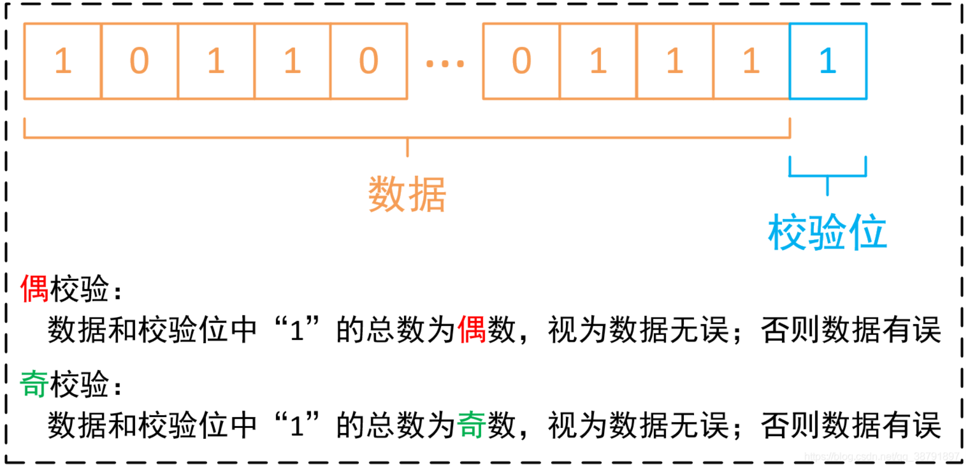
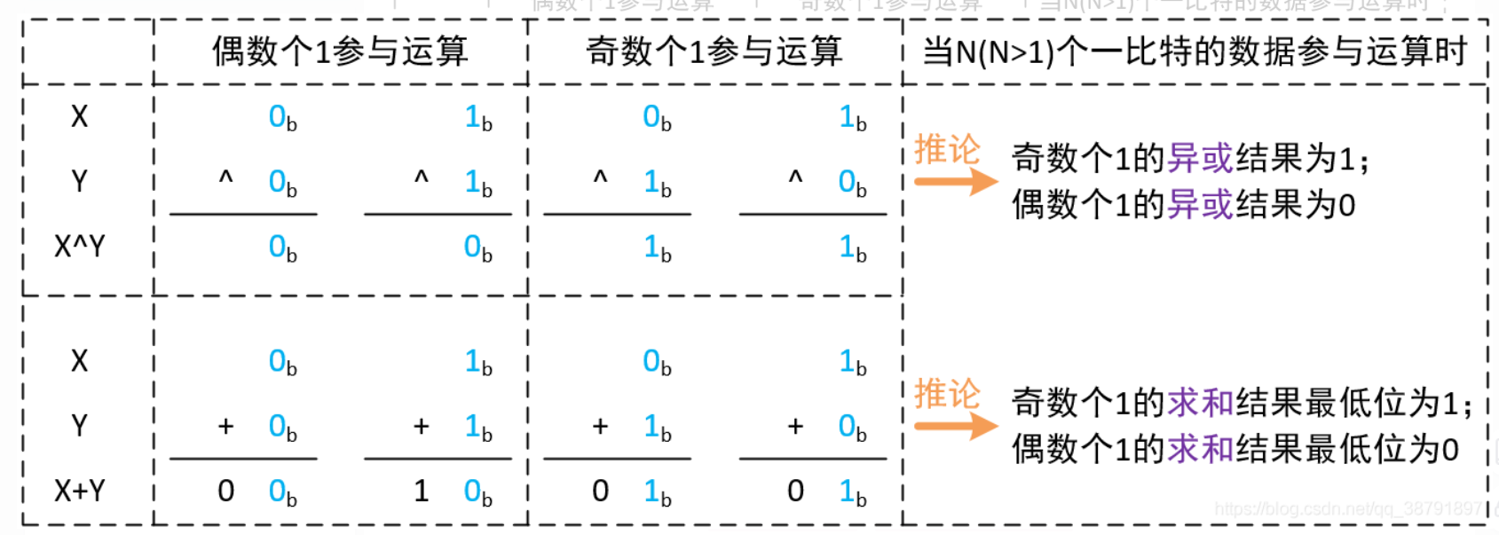
奇偶校验的定义如下图所示:
对数据做奇偶校验的Verilog模块代码如下:
module parity_check(
    input           clk,
    input           rst_n,
    input   [7:0]   data_in,
    output  reg     even_bit,
    output  reg     odd_bit
    );

    always@(posedge clk or negedge rst_n)
    begin
        if(!rst_n)
            begin
                even_bit <= 1'b0;
                odd_bit  <= 1'b0;
            end
        else
            begin
                even_bit <= ^data_in;   //偶校验需求下计算出来的校验位
                odd_bit  <= !(^data_in);//奇校验需求下计算出来的校验位
            end
    end

endmodule
测试模块
`timescale 1ns/1ps
module tb_parity_check;
    reg         clk;
    reg         rst_n;
    reg [7:0]   data_in;
    wire        even_bit;
    wire        odd_bit;

    always #10 clk = ~clk;

    initial
    begin
        clk   = 1'b0;
        rst_n = 1'b0;
        data_in = 10101001;
        #100 rst_n = 1'b1;

        repeat(1000)
            begin
                @(posedge clk);
                data_in = data_in + 1'b1;
            end

    end

    parity_check uut(
        .clk(clk),
        .rst_n(rst_n),
        .data_in(data_in),
        .even_bit(even_bit),
        .odd_bit(odd_bit)
    );
    endmodule
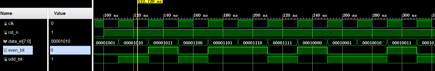
仿真结果图
最后
以上就是冷艳火龙果最近收集整理的关于Verilog中的奇偶校验的全部内容,更多相关Verilog中内容请搜索靠谱客的其他文章。
本图文内容来源于网友提供,作为学习参考使用,或来自网络收集整理,版权属于原作者所有。


![[EDA] 综合计时系统设计 【VHDL】一、实验要求:二、实验步骤分析:三、核心程序代码、仿真分析四、实验现象:五、部分程序源码:](https://www.shuijiaxian.com/files_image/reation/bcimg16.png)
发表评论 取消回复