目录
3.2 Sequential Logic
3.2.2 Counters
1. Four-bit binary counter
2.Decade counter
3. Decade counter again
4. Slow decade counter
5. Counter 1-12
6. Counter 1000
7. 4-digit decimal counter
8. 12-hour clock
3.2.3 Shift Registers
1. 4-bit shift register
2. Left/right rotator
3. Left/right arithmetic shift by 1 or 8
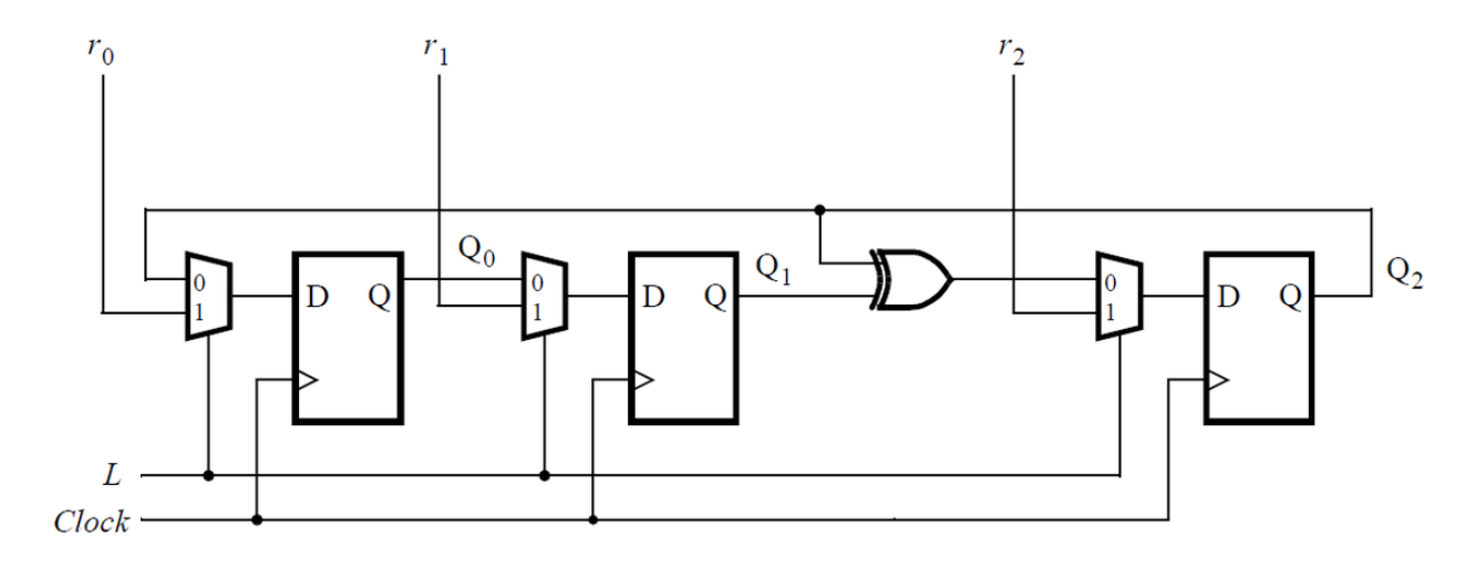
4. 5-bit LFSR
5. 3-bit LFSR
6. 32-bit LFSR
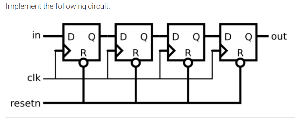
7. Shift register
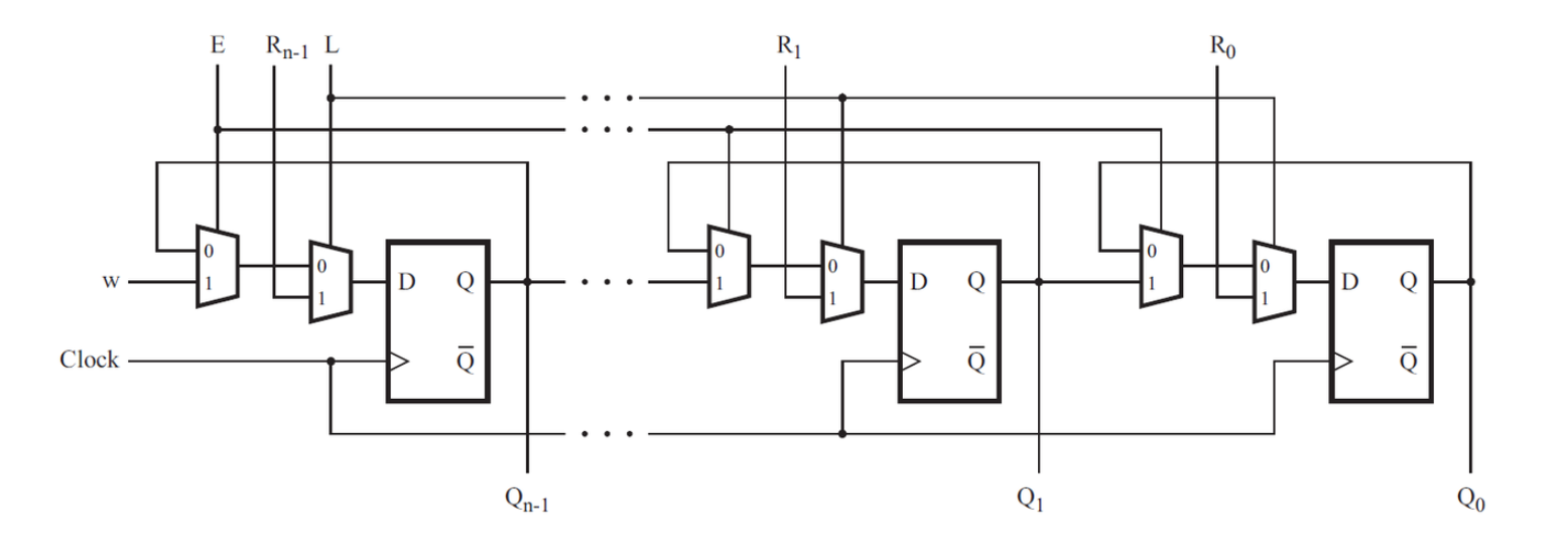
8. Shift register
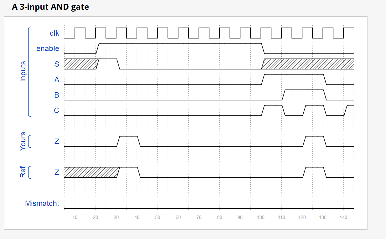
9. 3-input LUT
3.2.4 More Circuits
1.Rule 90
2. Rule 110
3. Conway's Game of Life 16x16
3.2 Sequential Logic
3.2.2 Counters
1. Four-bit binary counter
module top_module (
    input clk,
    input reset,      // Synchronous active-high reset
    output reg [3:0] q);


    always @(posedge clk)begin
        if(reset)begin
            q<='d0;
        end
        else begin
            q<=q+1'b1;
        end
    end

endmodule
2.Decade counter

module top_module (
    input clk,
    input reset,        // Synchronous active-high reset
    output [3:0] q);
    always @(posedge clk)begin
        if(reset) q<=4'd0;
        else if(q==4'd9) q<=4'd0;
        else q<=q+1'b1;
    end
endmodule
3. Decade counter again
Make a decade counter that counts 1 through 10, inclusive. The reset input is synchronous, and should reset the counter to 1.

module top_module (
    input clk,
    input reset,
    output [3:0] q);
    always @(posedge clk) begin
        if(reset) q<=4'd1;
        else if(q==10) q<=4'd1;
        else q<=q+1;
    end


endmodule
4. Slow decade counter
Build a decade counter that counts from 0 through 9, inclusive, with a period of 10. The reset input is synchronous, and should reset the counter to 0. We want to be able to pause the counter rather than always incrementing every clock cycle, so the slowena input indicates when the counter should increment.
module top_module (
    input clk,
    input slowena,
    input reset,
    output reg [3:0] q);

    always @(posedge clk)begin
        if(reset) q<='d0;
        else if(slowena &&q==9) q<='d0;
        else if(slowena) q<=q+1'b1;
    end

endmodule
5. Counter 1-12
Design a 1-12 counter with the following inputs and outputs:
-
Reset Synchronous active-high reset that forces the counter to 1
-
Enable Set high for the counter to run
-
Clk Positive edge-triggered clock input
-
Q[3:0] The output of the counter
-
c_enable, c_load, c_d[3:0] Control signals going to the provided 4-bit counter, so correct operation can be verified.
You have the following components available:
-
the 4-bit binary counter (count4) below, which has Enable and synchronous parallel-load inputs (load has higher priority than enable). The count4module is provided to you. Instantiate it in your circuit.
-
logic gates
module count4(
input clk,
input enable,
input load,
input [3:0] d,
output reg [3:0] Q
);
The c_enable, c_load, and c_d outputs are the signals that go to the internal counter's enable, load, and d inputs, respectively. Their purpose is to allow these signals to be checked for correctness.
module top_module (
    input clk,
    input reset,
    input enable,
    output [3:0] Q,
    output c_enable,
    output c_load,
    output [3:0] c_d
); //
    assign c_enable=enable;
    assign c_load=reset|(enable && Q==12);
    assign c_d=c_load?1:0;
    count4 the_counter (clk, c_enable,c_load, c_d,Q/*, ... */ );

endmodule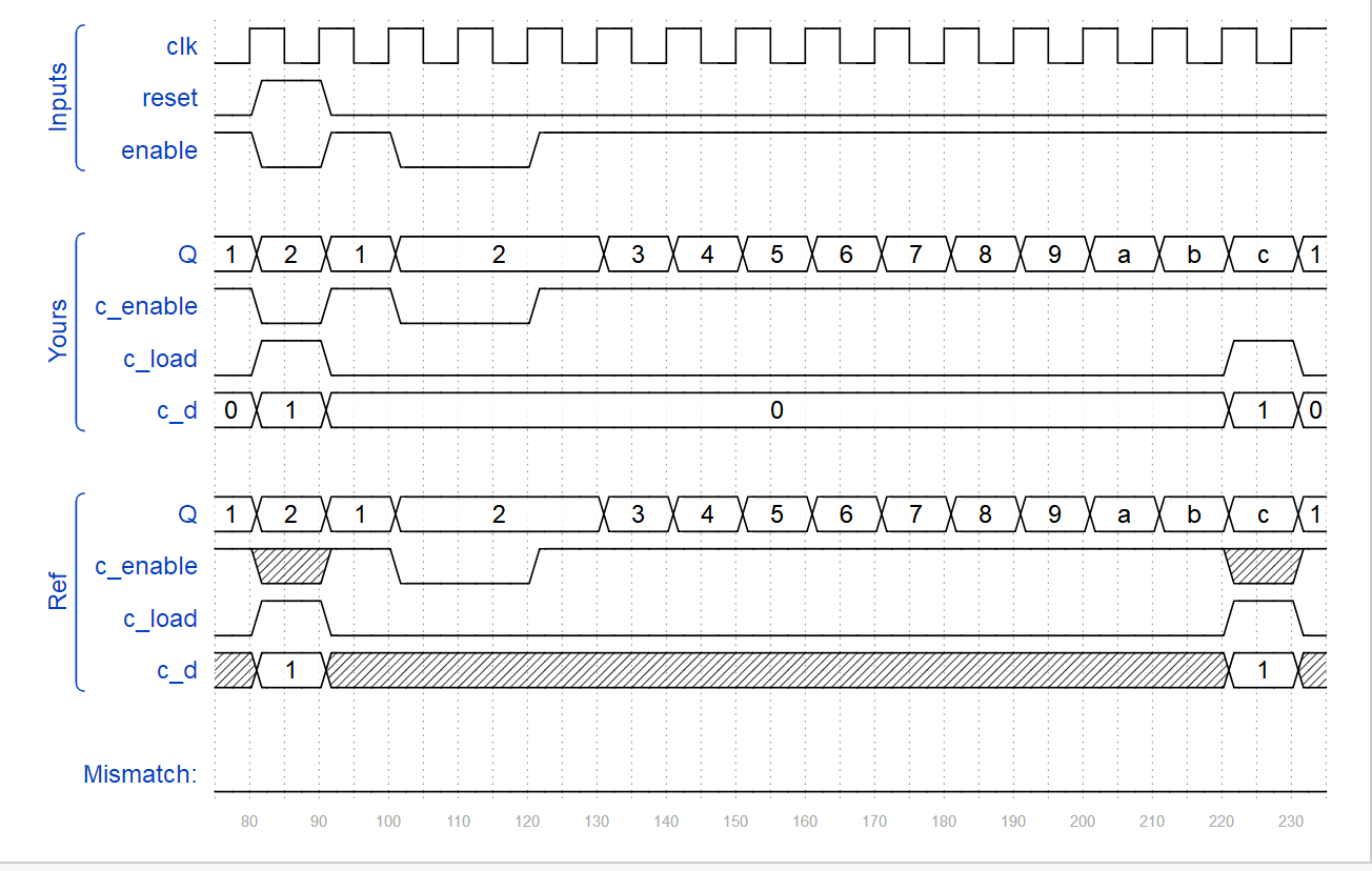
6. Counter 1000
From a 1000 Hz clock, derive a 1 Hz signal, called OneHertz, that could be used to drive an Enable signal for a set of hour/minute/second counters to create a digital wall clock. Since we want the clock to count once per second, the OneHertz signal must be asserted for exactly one cycle each second. Build the frequency divider using modulo-10 (BCD) counters and as few other gates as possible. Also output the enable signals from each of the BCD counters you use (c_enable[0] for the fastest counter, c_enable[2] for the slowest).
The following BCD counter is provided for you. Enable must be high for the counter to run. Reset is synchronous and set high to force the counter to zero. All counters in your circuit must directly use the same 1000 Hz signal.
module bcdcount (
input clk,
input reset,
input enable,
output reg [3:0] Q
);
module top_module (
    input clk,
    input reset,
    output OneHertz,
    output [2:0] c_enable
); //
    wire [3:0] q1,q2,q3;

    assign OneHertz=(q1==4'd9)&&(q2==4'd9)&&(q3==4'd9);
    assign c_enable ={q1==4'd9&q2==4'd9,q1==4'd9,1'b1};


    bcdcount counter0 (clk, reset, c_enable[0],q1/*, ... */);
    bcdcount counter1 (clk, reset, c_enable[1],q2/*, ... */);
    bcdcount counter2 (clk, reset, c_enable[2],q3/*, ... */);

endmodule
7. 4-digit decimal counter
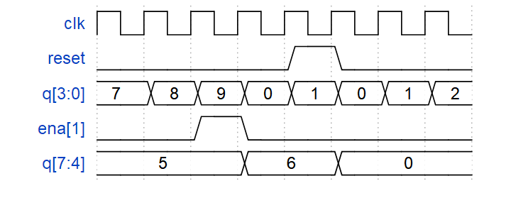
Build a 4-digit BCD (binary-coded decimal) counter. Each decimal digit is encoded using 4 bits: q[3:0] is the ones digit, q[7:4] is the tens digit, etc. For digits [3:1], also output an enable signal indicating when each of the upper three digits should be incremented.
You may want to instantiate or modify some one-digit decade counters.
module top_module (
    input clk,
    input reset,   // Synchronous active-high reset
    output [3:1] ena,
    output [15:0] q);

    always @(posedge clk)begin
        if(reset)begin
            q<='d0;
        end
        else begin
            if(q[3:0]!='d9)begin
                q[3:0]<=q[3:0]+1'b1;
            end
            else begin
                q[3:0]<='d0;
                q[7:4]<=q[7:4]+1'b1;
                if(q[7:4]=='d9)begin
                    q[7:4]<='d0;
                    q[11:8]<=q[11:8]+1'b1;
                    if(q[11:8]=='d9)begin
                        q[11:8]<='d0;
                        q[15:12]<=q[15:12]+1'b1;
                        if(q[15:12] == 4'd9)begin
                            q <= 0;
                        end
                    end
                end
            end
        end
    end


    assign ena[1]=(q[3:0] == 4'd9)?1:0;
    assign ena[2]=(q[7:4] == 4'd9 && q[3:0] == 4'd9)?1:0;
    assign ena[3]=(q[11:8] == 4'd9 && q[7:4] == 4'd9 && q[3:0] == 4'd9)?1:0;


endmodule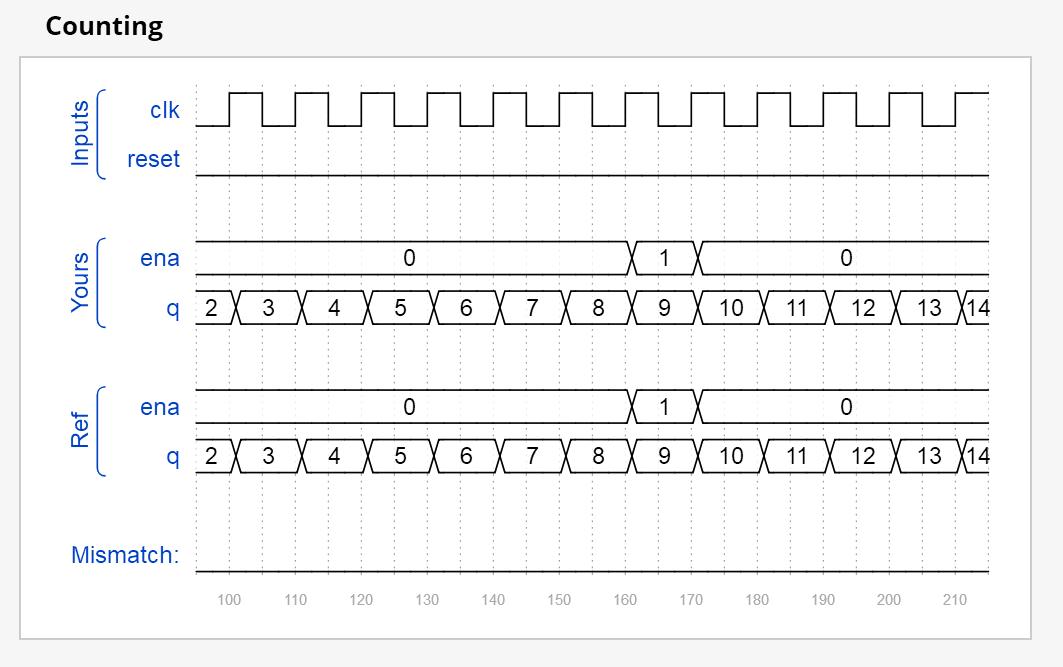
8. 12-hour clock
Create a set of counters suitable for use as a 12-hour clock (with am/pm indicator). Your counters are clocked by a fast-running clk, with a pulse on ena whenever your clock should increment (i.e., once per second).
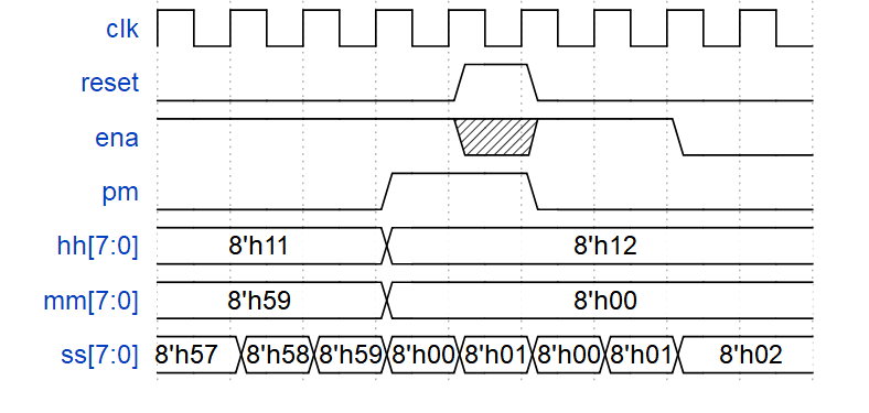
reset resets the clock to 12:00 AM. pm is 0 for AM and 1 for PM. hh, mm, and ss are two BCD (Binary-Coded Decimal) digits each for hours (01-12), minutes (00-59), and seconds (00-59). Reset has higher priority than enable, and can occur even when not enabled.
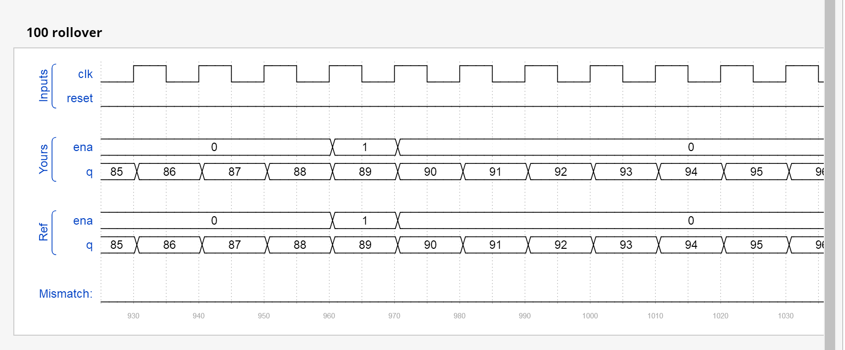
The following timing diagram shows the rollover behaviour from 11:59:59 AM to 12:00:00 PM and the synchronous reset and enable behaviour.
module top_module(
    input clk,
    input reset,
    input ena,
    output pm,
    output [7:0] hh,
    output [7:0] mm,
    output [7:0] ss);

    always @(posedge clk)begin
        if(reset)begin
            pm<=1'b0;
            hh[7:4]<=4'd1;
            hh[3:0]<=4'd2;
            mm<=8'h00;
            ss<=8'h00;
        end
        else begin
            if(ena==1)begin
                if(ss[3:0]!='d9)begin
                    ss[3:0]<=ss[3:0]+1;
                end
                else begin
                    ss[3:0]<=4'd0;
                    ss[7:4]<=ss[7:4]+1;
                    if(ss[7:4]=='d5)begin
                        ss[7:4]<='d0;
                        mm[3:0]<=mm[3:0]+1;
                        if(mm[3:0]=='d9)begin
                            mm[3:0]<='d0;
                            mm[7:4]<=mm[7:4]+1;
                            if(mm[7:4]=='d5)begin
                                mm[7:4]<='d0;
                                hh[3:0]<=hh[3:0]+1;
                                if(hh[3:0]=='d9)begin
                                    hh[3:0]<='d0;
                                    hh[7:4]<=hh[7:4]+1;
                                end
                                if(hh[7:4]=='d1&&hh[3:0]=='d1)begin
                                        pm<=~pm;
                                        hh[7:4]<='d1;
                                        hh[3:0]<='d2;
                                 end
                                if(hh[7:4]=='d1&&hh[3:0]=='d2)begin
                                        hh[7:4]<='d0;
                                        hh[3:0]<='d1;
                                end
                            end
                        end
                    end
                end
            end
        end
    end


endmodule
3.2.3 Shift Registers
1. 4-bit shift register
Build a 4-bit shift register (right shift), with asynchronous reset, synchronous load, and enable.
- areset: Resets shift register to zero.
- load: Loads shift register with data[3:0] instead of shifting.
- ena: Shift right (q[3] becomes zero, q[0] is shifted out and disappears).
- q: The contents of the shift register.
If both the load and ena inputs are asserted (1), the load input has higher priority.
module top_module(
    input clk,
    input areset,  // async active-high reset to zero
    input load,
    input ena,
    input [3:0] data,
    output reg [3:0] q);

   always @(posedge clk  or posedge areset)begin
        if(areset)
            q<=4'd0;
        else if(load)
            q<=data;
        else if(ena)
            q<={1'b0,q[3:1]};
        else
            q<=q;
    end


endmodule
2. Left/right rotator
Build a 100-bit left/right rotator, with synchronous load and left/right enable. A rotator shifts-in the shifted-out bit from the other end of the register, unlike a shifter that discards the shifted-out bit and shifts in a zero. If enabled, a rotator rotates the bits around and does not modify/discard them.
- load: Loads shift register with data[99:0] instead of rotating.
- ena[1:0]: Chooses whether and which direction to rotate.
- 2'b01 rotates right by one bit
- 2'b10 rotates left by one bit
- 2'b00 and 2'b11 do not rotate.
- q: The contents of the rotator.
-
module top_module(
    input clk,
    input load,
    input [1:0] ena,
    input [99:0] data,
    output reg [99:0] q);

    always @(posedge clk)begin
        if(load)
            q<=data;
        else if(ena==2'b01)
             q<={q[0],q[99:1]};
        else if(ena==2'b10)
             q<={q[98:0],q[99]};
        else
            q<=q;
    end

endmodule
3. Left/right arithmetic shift by 1 or 8
Build a 64-bit arithmetic shift register, with synchronous load. The shifter can shift both left and right, and by 1 or 8 bit positions, selected by amount.
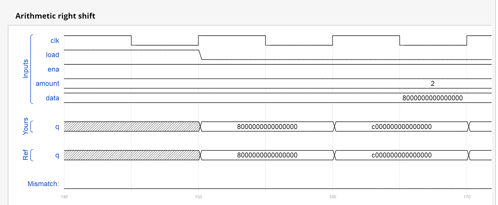
An arithmetic right shift shifts in the sign bit of the number in the shift register (q[63] in this case) instead of zero as done by a logical right shift. Another way of thinking about an arithmetic right shift is that it assumes the number being shifted is signed and preserves the sign, so that arithmetic right shift divides a signed number by a power of two.
There is no difference between logical and arithmetic left shifts.
- load: Loads shift register with data[63:0] instead of shifting.
- ena: Chooses whether to shift.
- amount: Chooses which direction and how much to shift.
- 2'b00: shift left by 1 bit.
- 2'b01: shift left by 8 bits.
- 2'b10: shift right by 1 bit.
- 2'b11: shift right by 8 bits.
- q: The contents of the shifter.
-
module top_module(
    input clk,
    input load,
    input ena,
    input [1:0] amount,
    input [63:0] data,
    output reg [63:0] q);
    always @(posedge clk)begin
        if(load)begin
            q<=data;
        end
        else if(ena)begin
            case(amount)
                2'b00:q<={q[62:0],1'b0};
                2'b01:q<={q[55:0],8'b00000000};
                2'b10:q<={q[63],q[63:1]};
                2'b11:q<={{8{q[63]}},q[63:8]};
                default: ;
            endcase
        end
        else begin
            q<=q;
        end
    end

endmodule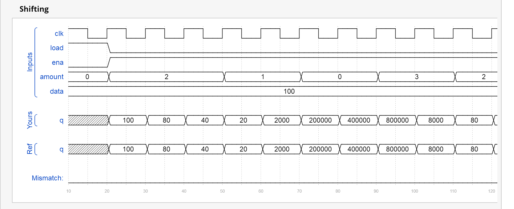
4. 5-bit LFSR
线性移位寄存器:
The following diagram shows a 5-bit maximal-length Galois LFSR with taps at bit positions 5 and 3. (Tap positions are usually numbered starting from 1). Note that I drew the XOR gate at position 5 for consistency, but one of the XOR gate inputs is 0.

module top_module(
    input clk,
    input reset,    // Active-high synchronous reset to 5'h1
    output [4:0] q
);
    always @(posedge clk)begin
        if(reset)begin
            q<='d1;
        end
        else begin
            q[0]<=q[1];
            q[1]<=q[2];
            q[2]<=q[3]^q[0];
            q[3]<=q[4];
            q[4]<=1'b0^q[0];
        end
    end

endmodule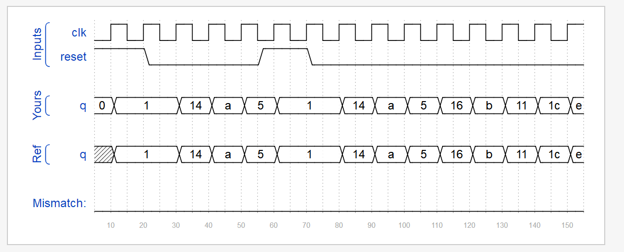
5. 3-bit LFSR
module top_module (
	input [2:0] SW,      // R
	input [1:0] KEY,     // L and clk
	output [2:0] LEDR);  // Q

    always @(posedge KEY[0])begin
        if(KEY[1])begin
            LEDR[2]<=SW[2];
            LEDR[1]<=SW[1];
            LEDR[0]<=SW[0];
        end
        else begin
            LEDR[2]<=LEDR[1]^LEDR[2];
            LEDR[1]<=LEDR[0];
            LEDR[0]<=LEDR[2];
        end
    end

endmodule
6. 32-bit LFSR
Build a 32-bit Galois LFSR with taps at bit positions 32, 22, 2, and 1.
module top_module(
    input clk,
    input reset,    // Active-high synchronous reset to 32'h1
    output [31:0] q
);
    always @(posedge clk)begin
        if(reset)begin
            q<=32'h1;
        end
        else begin
            q[0]<=q[0]^q[1];
            q[1]<=q[0]^q[2];
            q[2]<=q[3];
            q[3]<=q[4];
            q[4]<=q[5];
            q[5]<=q[6];
            q[6]<=q[7];
            q[7]<=q[8];
            q[8]<=q[9];
            q[9]<=q[10];
            q[10]<=q[11];
            q[11]<=q[12];
            q[12]<=q[13];
            q[13]<=q[14];
            q[14]<=q[15];
            q[15]<=q[16];
            q[16]<=q[17];
            q[17]<=q[18];
            q[18]<=q[19];
            q[19]<=q[20];
            q[20]<=q[21];
            q[21]<=q[0]^q[22];
            q[22]<=q[23];
            q[23]<=q[24];
            q[24]<=q[25];
            q[25]<=q[26];
            q[26]<=q[27];
            q[27]<=q[28];
            q[28]<=q[29];
            q[29]<=q[30];
            q[30]<=q[31];
            q[31]<=q[0];
        end
    end

endmodule
7. Shift register
module top_module (
    input clk,
    input resetn,   // synchronous reset
    input in,
    output reg out);

    reg q1,q2,q3;
    always @(posedge clk)begin
        if(resetn==1'b0)begin
            out<=1'b0;
        end
        else begin
            out<=q3;
        end
    end
     always @(posedge clk)begin
        if(resetn==1'b0)begin
            q3<=1'b0;
        end
        else begin
            q3<=q2;
        end
    end
     always @(posedge clk)begin
        if(resetn==1'b0)begin
            q2<=1'b0;
        end
        else begin
            q2<=q1;
        end
    end
     always @(posedge clk)begin
        if(resetn==1'b0)begin
            q1<=1'b0;
        end
        else begin
            q1<=in;
        end
    end


endmodule
8. Shift register
module top_module (
    input [3:0] SW,
    input [3:0] KEY,
    output [3:0] LEDR
); //
    MUXDFF mux1(KEY[0],KEY[1],KEY[2],KEY[3],SW[3],LEDR[3]);
    MUXDFF mux2(KEY[0],KEY[1],KEY[2],LEDR[3],SW[2],LEDR[2]);
    MUXDFF mux3(KEY[0],KEY[1],KEY[2],LEDR[2],SW[1],LEDR[1]);
    MUXDFF mux4(KEY[0],KEY[1],KEY[2],LEDR[1],SW[0],LEDR[0]);

endmodule

module MUXDFF (
 	input clk,
    input E,
    input L,
    input W,
    input R,
    output Q
);
    always @(posedge clk)begin
        if(L)begin
            Q<=R;
        end
        else begin
            if(E)begin
                Q<=W;
            end
            else begin
                Q<=Q;
            end
        end
    end


endmodule
9. 3-input LUT
In this question, you will design a circuit for an 8x1 memory, where writing to the memory is accomplished by shifting-in bits, and reading is "random access", as in a typical RAM. You will then use the circuit to realize a 3-input logic function.
First, create an 8-bit shift register with 8 D-type flip-flops. Label the flip-flop outputs from Q[0]...Q[7]. The shift register input should be called S, which feeds the input of Q[0] (MSB is shifted in first). The enable input controls whether to shift. Then, extend the circuit to have 3 additional inputs A,B,C and an output Z. The circuit's behaviour should be as follows: when ABC is 000, Z=Q[0], when ABC is 001, Z=Q[1], and so on. Your circuit should contain ONLY the 8-bit shift register, and multiplexers. (Aside: this circuit is called a 3-input look-up-table (LUT)).
module top_module (
    input clk,
    input enable,
    input S,
    input A, B, C,
    output Z );

   reg [7:0] Q;
    always@(posedge clk)begin
        if(enable)
            Q[7:0] <= {Q[6:0], S};
    end

    always@(*)begin
        case({A,B,C})
            3'b000:Z = Q[0];
            3'b001:Z = Q[1];
            3'b010:Z = Q[2];
            3'b011:Z = Q[3];
            3'b100:Z = Q[4];
            3'b101:Z = Q[5];
            3'b110:Z = Q[6];
            3'b111:Z = Q[7];
        endcase
    end
endmodule
3.2.4 More Circuits
1.Rule 90
Rule 90 is a one-dimensional cellular automaton with interesting properties.
The rules are simple. There is a one-dimensional array of cells (on or off). At each time step, the next state of each cell is the XOR of the cell's two current neighbours. A more verbose way of expressing this rule is the following table, where a cell's next state is a function of itself and its two neighbours:
| Left | Center | Right | Center's next state |
|---|---|---|---|
| 1 | 1 | 1 | 0 |
| 1 | 1 | 0 | 1 |
| 1 | 0 | 1 | 0 |
| 1 | 0 | 0 | 1 |
| 0 | 1 | 1 | 1 |
| 0 | 1 | 0 | 0 |
| 0 | 0 | 1 | 1 |
| 0 | 0 | 0 | 0 |
(The name "Rule 90" comes from reading the "next state" column: 01011010 is decimal 90.)
In this circuit, create a 512-cell system (q[511:0]), and advance by one time step each clock cycle. The load input indicates the state of the system should be loaded with data[511:0]. Assume the boundaries (q[-1] and q[512]) are both zero (off).
module top_module(
    input clk,
    input load,
    input [511:0] data,
    output [511:0] q );

    always @(posedge clk)begin
        if(load)begin
            q<=data;
        end
        else begin
            q<={1'b0,q[511:1]}^{q[510:0],1'b0};
        end
    end
endmodule
2. Rule 110
Rule 110 is a one-dimensional cellular automaton with interesting properties (such as being Turing-complete).
There is a one-dimensional array of cells (on or off). At each time step, the state of each cell changes. In Rule 110, the next state of each cell depends only on itself and its two neighbours, according to the following table:
| Left | Center | Right | Center's next state |
|---|---|---|---|
| 1 | 1 | 1 | 0 |
| 1 | 1 | 0 | 1 |
| 1 | 0 | 1 | 1 |
| 1 | 0 | 0 | 0 |
| 0 | 1 | 1 | 1 |
| 0 | 1 | 0 | 1 |
| 0 | 0 | 1 | 1 |
| 0 | 0 | 0 | 0 |
(The name "Rule 110" comes from reading the "next state" column: 01101110 is decimal 110.)
In this circuit, create a 512-cell system (q[511:0]), and advance by one time step each clock cycle. The load input indicates the state of the system should be loaded with data[511:0]. Assume the boundaries (q[-1] and q[512]) are both zero (off).
module top_module(
    input clk,
    input load,
    input [511:0] data,
    output [511:0] q
);

     always @(posedge clk) begin
         if(load == 1'b1)begin
            q <= data;
         end
        else begin
            q <= (q^{q[510:0],1'b0}) | (~{1'b0,q[511:1]}&{q[510:0],1'b0});
        end
    end
endmodule
3. Conway's Game of Life 16x16
最后
以上就是超级小松鼠最近收集整理的关于HDLBits 系列(7)——Sequential Logic(Counters、Shift Registers、More Circuits)3.2 Sequential Logic的全部内容,更多相关HDLBits内容请搜索靠谱客的其他文章。


发表评论 取消回复