It's a Buck; It's a Boost, No! It's a Switcher!
Sanjaya Maniktala, National Semiconductor Corp., Santa Clara, CA
We like to give everything a name or label very quickly. We probably feel we can then easily identify the object in the future, and also point it out knowledgeably to others: 'look it's a Buck, it's a Boost, it's a Buck-Boost'. In fact, as this article points out, especially when we come to integrated regulator ICs like National's "Simple Switcher" lineup, it pays to keep in mind that these are first and foremost Switcher ICs. They can lend themselves to various other applications beyond their primary intended function. So by labeling an IC as a Buck or a Boost IC right off the bat, we may just be missing several other opportunities.
A switchmode IC can actually be used across other topologies quite freely. For example a Buck IC can be used in a Buck-Boost application and vice-versa. This is not so puzzling once we understand that a switcher is just that: it basically switches a transistor between ON and OFF states. How we use the transistor and configure our circuit to switch a voltage across an associated inductor and how we finally route the energy to the output is not necessarily fixed. Indeed there are limitations on what all we can do, but that has more to do with how the transistor is actually driven, how the internal control of the IC is referenced, etc. It is certainly important to understand the internal construction of the IC itself, but to finally see the other 'hidden' applications needs a better (and more abstract) understanding of switcher topologies themselves.
Related literature occasionally refers to some of these hidden applications, but in a rather scattered and unintelligible way. One major problem we noticed was the way a schematic is often drawn. We came across schematics that required several right angle turns and/or several horizontal and vertical mirror reflections to make any sense of. Unless of course the IQ of the reader was genius cubed. To compound the confusion, there was rarely any attempt to even explicitly state the fact that the underlying topology had changed. In the accompanying text, it may just have been mentioned in passing that the Buck IC was being used in an 'inverting' configuration (or a 'positive to negative' converter). Go figure! What is the maximum load current in this new configuration and what is the safe input operating voltage range? Why are these different now? Is that the feedback? And how does it really work? Is the output regulation as good as it was for the original Buck? Questions like these just add to the general mystery surrounding the host of other possible applications for switchers, and to the general misery of the designer. And thereby effectively stymie the exploration of these extra possibilities.
This article tries to outline the many possible hidden uses of integrated switchmode power supply ICs, particularly the "Simple Switcher" lineup from National, in a clear, concise and complete way. The average designer will have no trouble in extending the same principles to all related switcher applications, even those using controllers to drive external switches.
What is 'Ground'?
We need to start with some basics. In a DC-DC converter there are two input rails (connected to the DC source) and two output rails (connected to the load). Of these, one rail is always shared between the input and the output. By convention, this common rail is designated the (system) ground. It is therefore the ground for the power stage. But there is another 'ground'. This is the IC/control ground. This may or may not always be connected to the system ground, especially if the IC is being used in a manner other than its primary intended application. So if we connect the grounds differently, there could be are other possible problems. These are mentioned briefly here at the outset because even though they are not central to the focus of this article, these may be of related importance as we explore the hidden applications, and may thus need to be solved.
a) The feedback path may not be direct anymore. The feedback voltage to the control always needs to be referred to the IC ground. But since this system ground may be at a different level voltage sensing of the output would now need to be differential in nature. Then this difference needs to be level-shifted or 'translated' to the IC ground. There are several standard ways of doing this, all involving external components, and these will be discussed later.b) Any ON/OFF control if required will also need to be indirectly implemented for the same reason. But the variations are extremely diverse. For example, some ICs turn the PWM stage ON if the voltage applied on the ON/OFF pin is positive (with respect to the IC ground), but in some cases the ON/OFF pin needs to be connected to IC ground to be activated. In addition the ON/OFF pin usually has a voltage rating which should not be exceeded. Therefore, the designer is going to have to independently figure out the best way to implement ON/OFF control in such cases. Of course he may not even require to turn OFF the IC, and that would be easy to do if not automatic. In this article we are not going to delve into this ON/OFF aspect further.
Note: The feedback pin also has maximum voltage ratings that should not be exceeded. Though this pin is inherently self-stabilizing, at least in steady state, the designer may need to watch out for transients during start-up or shutdown or under short circuits on the output that could damage the feedback pin. This is of concern only when the IC is used 'unconventionally', i.e. in a configuration other than its basic intended application.
Since the many different configurations can appear bewildering at first sight, it will help to point out their common threads. This will lead to a better visualization in terms of their basic building blocks and highlight all the things we can do without missing any possibilities. Therefore we will start off by some basic definitions.
Definitions: N-switch/P-switch
For bringing the myriad possibilities under smaller umbrellas, we need to make some rather unconventional definitions in this article. The reader should bear with us, as he will see that it really does help in isolating the common threads among the various hidden applications.
In Figure 1a we have indicated that a voltage of magnitude 'v' needs to be applied with respect to the Source terminal of both N-channel FETs and P-channel FETs to turn the FET ON (assuming enhancement types only). The dotted triangles (alongside the label 'v') indicate the direction of increasing voltage (in terms of magniude). We have also indicated that a voltage of magnitude 'v' needs to be applied with respect to the Emitter terminals of both NPN and PNP BJTs ('Bipolar Junction Transistor') to turn the BJT ON.
Throughout this article we will usually attempt to keep the lower voltage input rail on the bottom side of the figure and the higher voltage input rail on the top side. Further, the input is on the left side and the output on the right. These steps will help in keeping all the schematics visually appealing, easy to follow, and mutually consistent.
In Figure 1b we have show the easiest way to turn the FET or BJT OFF is to connect the gate/base to the Source/Emitter.
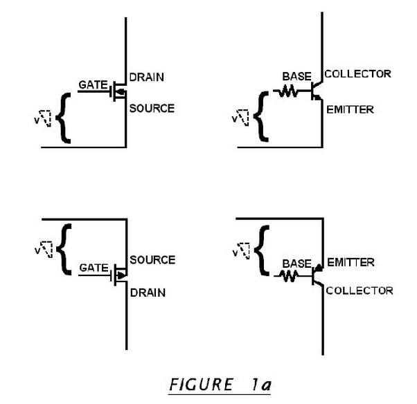
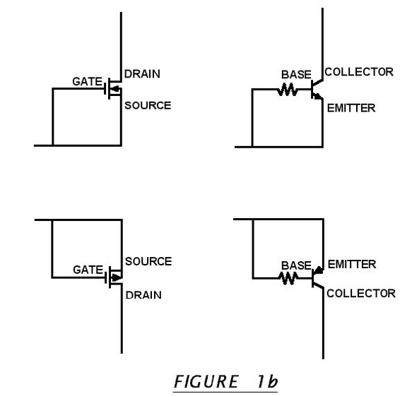
Because of the drive similarities, in this article we will generally talk in terms of an 'N-switch' (being either an N-channel FET or an NPN BJT) or a 'P-switch' (either a P-channel FET or a PNP BJT.
Another Definition: The 'LSD' cell
With no hallucinogenic properties at stake, the LSD cell as defined here goes a long way in understanding which hidden applications are a 'natural possibility' for a given IC and which are not. It will be shown that if we identify the LSD cell type occurring in the original intended function of a switcher IC, we can easily apply it to any other topology in which the same LSD cell type occurs, irrespective of the topology. We will also see that in some cases, by a special technique we can even make an IC perform in an LSD cell type other than its originally intended LSD cell. This is a clear alternative to talking in terms of Buck or Boost cells, which is more common in related literature. The justification here is that LSD cells, not Boost/Buck cells, are the key to understanding and tracking down the hidden applications. The topology can always change but not the LSD cell type! And this will be borne out soon.
Coming to the basic structure of power conversion circuits, in all cases we have an inductor (L), a switch (S) and a diode (D) connected to each other. This is hereafter generically nicknamed an 'LSD cell'. We will see that we can have in all just 4 LSD cell types. Two correspond to N-switches, and two to P-switches.
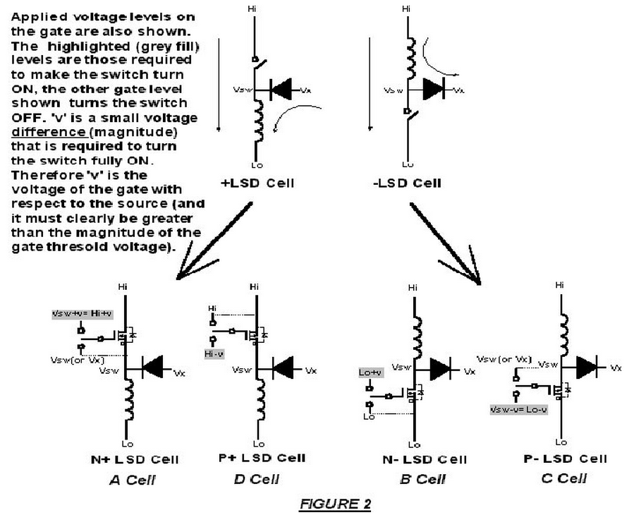
LSD cell types are shown in Figure 2 (the internal details of the switch are not shown here). When the switch turns OFF the current freewheels through the diode. Therefore the direction of the diode must be as indicated for each case. The 'LSD node' (the common node between the three components) is also called the 'switching node' ('Vsw') as in normal power conversion terminology. Therefore the two main cases are
The cathode of the diode connects to the LSD node: call it a '+' LSD cell The anode of the diode connects to the LSD node: call it a '-' LSD cell
For each case above, we can have either an N-switch or a P-switch. Therefore, in all we have four basic LSD cells at the root of any power converter. We will give these names Type A, B, C and D.
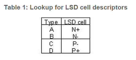
Type A: N+ cell: cathode is LSD node, N-channel FET or NPN BJT Type B :N- cell: anode is LSD node, N-channel FET or NPN BJT Type C : P- cell: anode is LSD node, P-channel FET or PNP BJT Type D : P+ cell: cathode is LSD node, P-channel FET or PNP BJT
This is also provided in the lookup table, Table 1.
We introduce the following terminology from Figure 2. We need to do this because when we come to 'configurations' of the topologies we will see that the labeling of the rails keeps changing. The system 'ground' may be re-designated based on the common rail criterion discussed earlier. Therefore it is important to visualize the configurations in which the cells find themselves in, in terms of a higher voltage rail and a lower voltage rail rather than a specific label.
a) The higher voltage potential is called 'Hi' (note it is on the top side of the figure). b) The lower voltage potential is called 'Lo' (note it is on the bottom side of the figure). c) The common node shared by the switch, the diode and the inductor is 'Vsw' and is the 'switching node'. This voltage on this node is always 'swinging'. d) The voltage on the other side of the diode is a DC level in all cases and it is called 'Vx' here. Therefore Vsw will equal Vx during the time the switch turns OFF, because the diode must then conduct. When a diode conducts it can be mentally thought of as 'connecting' its two terminals together. So during the entire switch OFF-time Vsw=Vx (ignoring the small forward voltage drop across the diode, and assuming continuous conduction mode). Therefore we can again refer to Figure 2 and notice that it is indicated that one way to turn the switch OFF is to connect the Gate/Base to Vx (rather than to Vsw).
Note: This implies that the 'ground pin' of control ICs can often be permanently connected to the point Vx. In some cases Vx is the output voltage rail itself. We will see this principle in action in a succeeding section.
Configurations of Switching Regulator Topologies
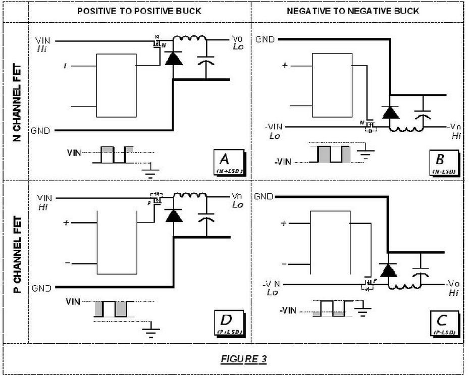
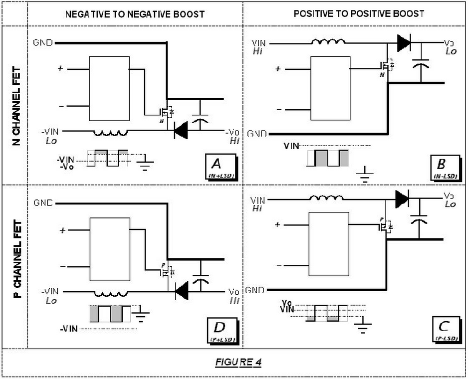
We note that the words 'Boost', or 'Buck' or 'Buck-Boost' always refers only to the magnitudes of the input and output voltages. So now we see the need for qualifiers like 'negative to negative', 'negative to positive' etc. to fully describe the actual configurations. The negative (or inverted) form of the modern positive to positive Boost converter is in full a 'negative to negative Boost converter'. It would convert say -12V to -48V relative to the (common) ground rail.
We have four possible configurations for each of the standard topologies. In Figure 3, Figure 4 and Figure 5 we show the possibilities for the Buck, the Boost and the Buck-Boost converters respectively. Note that we can now relate what Hi, Lo, Vsw, Vx levels really refer to in the schematic, in terms of actual circuit labels for the rails. The gate drive levels are also shown. As in Figure 2, the highlighted areas of the gate drive (gray fill) are where the FET is ON. Otherwise it is OFF. It is also indicated whether they belong to Types A, B, C or D, as defined previously.

N-Switch Configurations to P-Switch Configurations
We saw above that there are different possible 'configurations' of a given topology. This means that though it does not amount to a fundamental (or topological) change, this does change the schematic significantly.
Nowadays it is customary to call the lower input rail as the system 'ground' ('negative ground' convention). But for many years it was commonplace to refer to the upper rail as the ground ('positive ground'). Though there are some practical EMI vs. thermal management tradeoff issues also related to the typical switch/diode structures, it is almost by sheer tradition that many telecom systems are still 'positive ground'. We initially feel that in going from a positive ground schematic to a negative ground schematic, it may just be a simple matter of re-labeling in terms of which rail we decided to call 'ground', i.e. the upper input rail or the lower input rail. But when we consider the fact that there is a common rail between the output and the input of a switching converter, and it is this rail that needs to be the designated the 'ground' all the way from the input to the output, we realize that the circuit schematic really needs to change.
Yet engineers learnt quickly to do so. The method to proceed is an old one: to draw the ground negative circuit from a ground positive circuit (and vice versa) we simply invert all circuit polarities. So '+' becomes '-' and 'hi' becomes 'lo' (and vice versa respectively). And for example the anode (positive terminal) and cathode (negative terminal) of a diode are interchanged, which is equivalent to just reversing the direction of the diode. See Figure 6 for an example of how to 'invert' various components (shown with some typical voltage levels). Note in particular how a switch is inverted. The pin assignments are NOT changed (Drain is still a Drain etc.), but the structure is inverted (for example from an N-channel FET to a P-channel FET).
In Figure 7 we perform 'inversion' on a N+ Buck circuit (type A) and show that it leads directly to a P- Buck circuit (type C). If it is not so obvious, we can flip the circuit vertically ('reflection') to put it in line with our declared goal of visualizing all circuits with higher input voltage rails on the top side of the page and lower voltage rails on the lower side. Comparing it with Figure 3 we will see that indeed we have generated not only the P- circuit but also the required gate drive levels.

Therefore in all cases (for any topology), 'inversion' amounts to changing the LSD descriptor as follows:
N > P + > -
In terms of the simplified lookup table for Types a, B C and D, inversion would amount to changing the configuration type (for any given topology) according to:
A > C B > D
This implies that if we study the more common N-switch configurations we can quickly generate the corresponding inverted P-switch version (and vice versa if we wish).
Example1: If we need to create a schematic for a negative to positive Buck-Boost using a P-channel FET (Type C from Figure 5), we can start by generating a positive to negative Buck-Boost schematic using an N-channel FET (Type A from Figure 5) and then invert it.
Keep in mind that N-switches are generally preferred as they reduce die size for a given Rds/Vce_sat as compared to P-switches. Therefore we will now focus exclusively on IC's using N-switches only.
As mentioned in the Introduction, it is important to also note the internal construction of the switcher IC. Since we are ignoring P-switches hereafter, our focus has in effect shifted entirely to N+ (Type A) and N- (Type B) LSD cells only, because we now know that C can be generated from A, and D from B.
Returning to Figure 3, Figure 4 and Figure 5, we see that the details of the control were not shown. In addition though the switch is shown outside the square block, it can be considered integrated into the IC. This is typical of National's Simple Switcher series. Let us now study typical integrated ICs first to see how they are internally configured.
Commonly, there are four basic Switcher IC types available (all use N-switches) as shown in Figure 8. On closer examination, we see that these fall into two basic categories, hereby designated Type 1 and Type 2. Note the bold trace shown in the figures is the connection trace between the switch and the control. And this is what makes the two types really different. Type 2 ICs are generally considered 'Flyback/Buck-Boost/Boost' ICs and Type 1 ICs are considered 'Buck ICs'. We will see that Type 1 ICs are generally the most versatile. Therefore we will discuss the various possibilities using a Type 1 IC first and later take up Type 2.

Before we go on let us briefly summarize some key observations from Figure 8.
* Type 1 connects the Source/Emitter (lower voltage switch pin) to the - pin of the control block.
* Type 2 connects the Drain/Collector (higher voltage switch pin) to the + pin of the control block.
* NPN switches are generally easier to drive since the Base has to be taken only slightly higher than the Emitter to turn the switch ON (note that even the small existing CE drop can be used for this purpose, as in Darlington/beta (gain)-multiplier drive arrangements).
* In Type 1 ICs, the Source/Emitter of the switch is connected to the 'GND pin' (lower rail) of the IC (the '-' pin). The slight positive bias voltage required to turn ON the switch can be easily derived by stepping down the voltage available at the '+' supply pin of the IC.
* Therefore a FET-based Type 2 is the hardest to drive. We must recognize that when the switch turns ON, the Source/Emitter pin becomes (almost) equal to the '+' supply pin. But to keep the FET ON, a voltage higher than the IC supply pin is required (typically 5-10 Volts higher depending on type of FET). This is not readily available as it is outside the range of the input supply rails. In fact there is no other easy way other than to bootstrap the driver stage, such that the driver floats on the switching node.
* Note that the actual 'SW' pin labeling in Figure 8 depends on the perceived application for the part, not necessarily on how it is actually used. It cannot always be assumed that the 'SW' pin is the switching node of the regulator power stage. In Figure 8 the SW pin is simply the uncommitted pin of the transistor, i.e. the one NOT directly connected to either the '+' or '-' pins (going to the supply rails). Under 'normal' expectations, it is expected to be the switching node (as it has the required degree of freedom to 'swing'). But in fact this may not be always true. As we will see later, this pin can be connected to a fixed rail, and in fact either the '+' or '-' pins may be forced to be the swinging/switching node! We had also seen earlier that the '-' pin (IC ground for negative ground schematics), may not be the system ground either. Therefore in all cases, the designer needs to take the labeling of the IC pins with a pinch of salt, never forgetting what they really are in terms of the internal construction of the IC.
* In all cases the feedback node is referred by the control to the lower ('-') rail of the IC. But in reality, how the output voltage of the converter is actually sensed and the voltage 'translated' so as to reference it correctly to the IC control, depends on the actual application the IC is being used for. This will be discussed later.
* Type 1 ICs usually have two voltage ratings: one for the control ('+' pins in Figure 8) and a higher rating for the switch (Drain/Collector), both measured with respect to the IC ground (the '-' pins in Figure 8).
* Type 2 ICs almost invariably do not permit the 'SW' pin to be taken more than 1V below IC ground. This limits some possible applications, particularly some 'clever' ideas using tapped inductors (which very few seem to need or want).
Now we will take up Type 1 and Type 2 ICs in more detail below.
Flyback/Buck-Boost/Boost ICs
These are generically referred to as Type 1 ICs in this article. We will now see why there is no essential difference between an IC intended primarily for a Boost application and one say for a Flyback/Buck-Boost application. We should first be aware of the basic topological difference between a Boost and a Buck-Boost power stage.
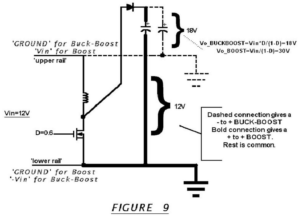
In Figure 9 we can see that the change from a 'positive to positive' Boost to a 'negative to positive' Buck-Boost is actually very simple: it involves just re-directing the connection of the negative terminal of the output capacitor from the 'lower rail' to the 'upper rail'. Therefore the two topologies are not all that different. In fact as far as the drive of the switch is concerned it sees absolutely no difference between these topologies, because basically only the designation (or labeling) of the rails has changed. The output voltage rail is exactly 30V above the IC ground (not system ground) in both cases (for the same duty cycle). So the IC doesn't know better.
The main difference is in the feedback. Since for a Boost, the IC control is typically always connected to the 'lower rail', a simple resistive divider across the output capacitor can be used to connect directly to the feedback pin of the IC control. But for the Buck-Boost, the output voltage is with respect to the system ground (the 'upper rail'), whereas the IC control is still referenced to the 'lower rail'. Therefore a more elaborate solution is required. This usually takes the form of a differential amplifier stage to sense the output voltage of the Buck-Boost and then to 'translate' it to the lower rail. But the requirements, specifications and ratings of such a differential stage are so diverse depending on the input/output levels that this extra stage is rarely (if ever) integrated into the switcher IC. This means that a 'true Buck-Boost integrated switcher' (with integrated feedback) may be near impossible to find. So, since the feedback implementation is generally external to the IC, there is no remaining architectural difference left between a 'Boost IC' or a Buck-Boost IC'. They are one and the same. It is no surprise that any switcher meant for a Flyback/Buck-Boost application can always successfully be used for a Boost application and vice versa.
In this article we will use the word 'Flyback' to refer exclusively to a Buck-Boost stage with inherent primary to secondary isolation. Obviously this requires a transformer. But we could also have a transformer-based Buck-Boost with no isolation present, because the primary and secondary windings are connected together for easier implementation of feedback. However, in both cases the feedback method involves using two resistors in a divider network positioned at the output, and no differential amplifier stage is required.
Coming back to the main focus of this article, we now see the other possible applications of a Flyback/Boost IC.
Flyback/Buck-Boost/Boost IC Applications
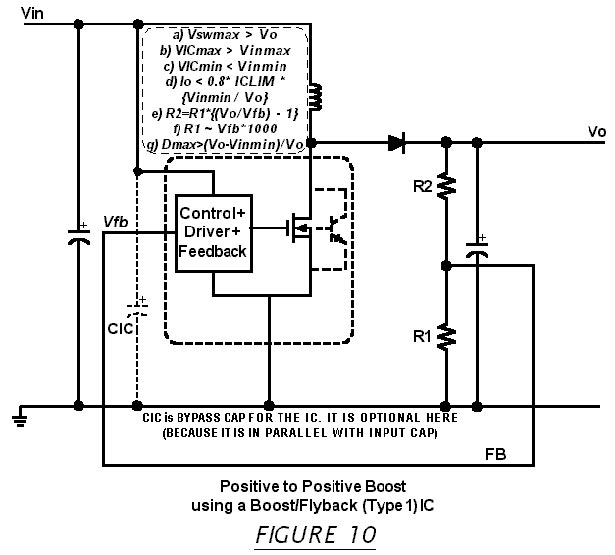
This is the IC shown as 'Type 1' in Figure 8. It can be used for all the applications presented below. For more details and a summary, view these figures along with the description and comments in the Table 2. This Table is also repeated as Table 3 in Part 2 of this article. Note that this table features only the transformer-less configurations, and also the Type 2 configurations are grayed-out in Part 1, as these will be discussed in Part 2. Note that for convenience, in all cases the main design equations are also provided within the figures themselves. They provide the required ratings of the SW pin (Vswmax), the IC/control pin (VICmax) (both measured with respect to the IC ground pin), and the maximum load possible (based on the set current limit of the switch 'ICLIM'). The maximum load current requires choosing inductance correctly.A current ripple ratio 'r' of 0.4 or less must be the target. Refer to AN-1197 and AN-1246 at http://power.national.com for more details.
Some of the configuration conditions/equations may depend on the minimum and/or maximum input voltages, Vinmin and Vinmax respectively. In addition, every controller is designed with a certain maximum possible duty cycle limit 'Dmax'. Clearly, if the input and output voltages demand more than 'Dmax' the circuit cannot work. Therefore the equation to check this possible limitation is also provided. The feedback scheme is also shown, and the equations to set the resistor values are also provided. 'Vfb' is the voltage on the feedback pin of the IC under regulation (for example it is the reference voltage to the internal error amplifier for an Adjustable output part). National's switcher ICs generally come either as 'Adjustable', requiring an external resistive divider to set output, or Fixed voltage parts, where the divider is internal to the IC.
In all the equations to follow, the switch and diode forward drops are generally assumed to be negligible. So a little additional guardbanding may be necessary to take these into account.
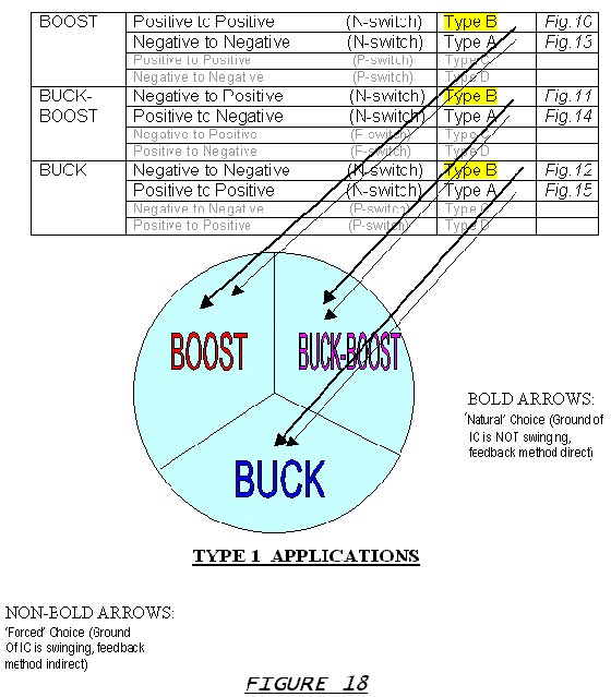
Now the crucial chain of logic behind hidden applications: the primary intended application for this IC is the positive to positive Boost. We can discover that this involves a 'N-' cell (Type B). Therefore we conclude that this IC is most 'comfortable' with any topology/configuration, provided it involves a (similar) Type B cell. This cell is a 'natural choice' for this IC. Note that we also start seeing the advantage in talking in terms of LSD cells rather than directly in terms of topologies/configurations. This common thread would have been missed in that case.
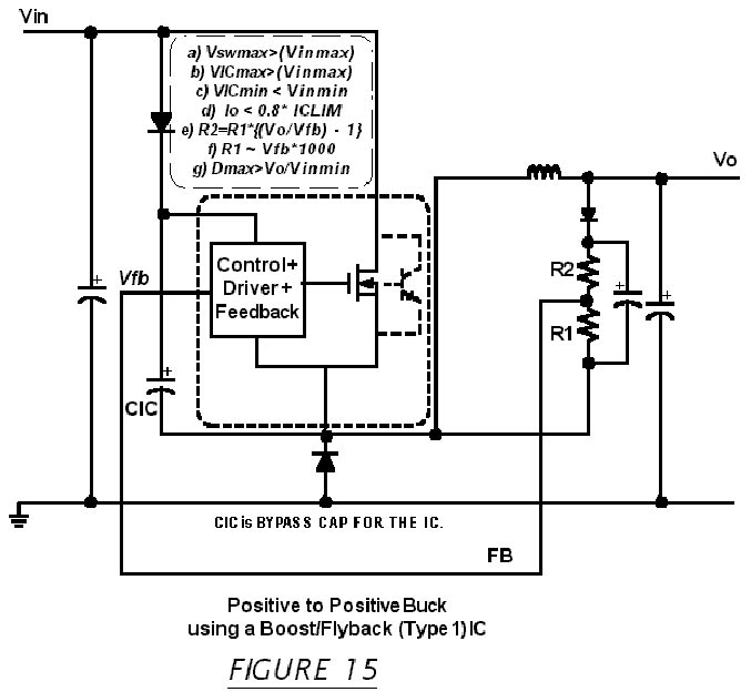
The only other possible cell choice using an N-switch is the Type A (N+) cell. Topologies/configurations requiring a Type A cell are therefore considered a 'forced' choice for a Type 1 IC. They can be implemented using a common underlying technique that involves floating the IC ground on the switching node and then doing a peak detect for implementing feedback. This will be described later.
Now we go through the figures one by one.
a) Positive to Positive Boost: Uses a Type B cell. The primary intended Application for a Type 1 IC. See Figure 10. Uses a simple resistive divider to implement feedback.
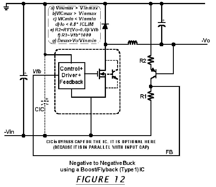
b) Negative to Positive Buck-Boost: Uses a Type B cell. Another intended Application for a Type 1 IC. See Figure 11. Note the 'cheap and dirty' differential output sense and voltage translation (actually a simple voltage-dependent current source) using a single PNP transistor. Note that 0.6V is assumed for the Vbe drop. Therefore the output regulation is not very accurate. Later more accurate differential op-amp techniques are presented, but they need an external supply rail to power them.
c) Negative to Negative Buck: Uses a Type B cell. See Figure 12. Note the 'cheap and dirty' output voltage sense technique as in Figure 11. Therefore the output regulation is not very accurate again. Differential op-amp techniques can be used instead for higher accuracy.
d) Negative to Negative Boost: Uses a Type A cell. A 'forced' application by definition. See Figure 13. Here the fact that the Drain/Collector is not connected to the input of the control section is exploited. The IC ground floats on the switching node (this can cause higher EMI). Peak charge feedback technique is used.Here a (near) copy of the output voltage is created by peak charging a small capacitor connected between the switching node (IC ground) and the output ground, via a diode. Note that because of the diode drops this is an inaccurate method. Some techniques to compensate for this error are available, but in general: The output regulation for any topology/configuration which uses a cell which is not the same as the cell for the IC's primary intended application is always inherently inaccurate. We will also later see that in Type 2 IC's such 'forced' applications are not even possible due to the due to the fact that the input to the switch (power stage) and the input to the IC (control section) are not separated out as in Type 1 ICs.
e) Positive to Negative Buck-Boost: Uses a Type A cell. A 'forced' application by definition. See Figure 14. Therefore again, inaccurate peak detect feedback technique must be used and this sub-circuit is again between the switching node and output ground. The IC floats on the switching node (this can cause higher EMI).
f) Positive to Positive Buck: Uses a Type A cell. A 'forced' application by definition. See Figure 15. Therefore again, inaccurate peak detect feedback technique must be used and this sub-circuit is now between the switching node and output rail. The IC floats on the switching node (this can cause higher EMI).
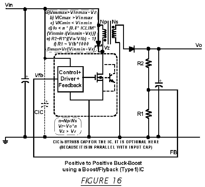
In addition to the inductor based topologies above, we could use transformers to 'correct' the polarity reversal of a buck-boost. This helps in implementing feedback too. With transformers, we could have primary to secondary isolation or no isolation. For completeness sake we present these variations too here.
g) Positive to Positive Buck-Boost: This involves a transformer with no isolation. See Figure 16.
h) Positive to Positive Flyback: This involves a transformer with primary to secondary isolation. An external voltage reference is used with an opto-transistor to regulate. See Figure 17.
Figure 18 summarizes all the inductor-based possibilities. The P-switches are grayed out as it was indicated earlier how they can be derived by inverting N-switch configurations. The N-switch configurations with a 'natural' cell choice (Type B LSD cell) are shown with bold arrows and yellow highlighting. The non-bold arrows are possible forced choices involving peak detect feedback method and swinging IC ground, and all use Type A LSD cells.


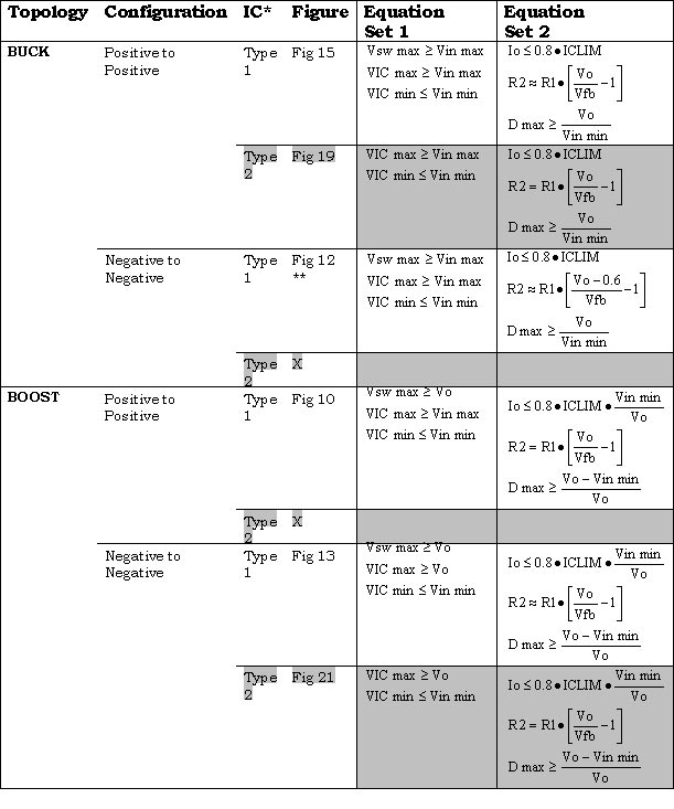

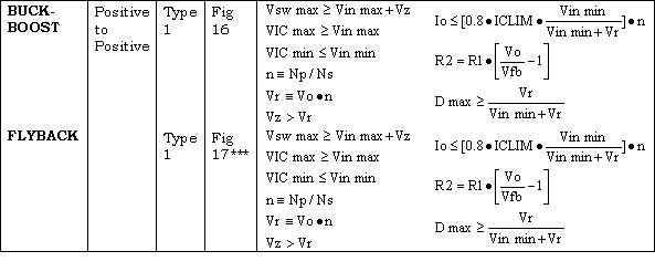
Note: By convention, R2 is always connected to the higher voltage rail of output and R1 to the lower.
*Type 1 IC is a 'Boost/Buck-Boost/Flyback IC'. Type 2 IC is a 'Buck IC'.
** For Figure 11 and 12, accurate differential amplifier sensing can be used: see Table 3 in the next Part of this article.
*** Vfb is NOT the voltage on feedback pin of IC in Figure 17. Also, set zener voltage Vz significantly higher than Vr (typically 20-30% higher) to minimize losses in zener and to maximize efficiency.
Conclusion of Part 2
In the next part we will cover applications using Type 2 (Buck) ICs. Improved techniques for implementing feedback using differential sensing will also be presented. Several worked examples will be provided using National's integrated switcher lineup. And finally some subtleties that must be kept in mind as we traverse topologies will also be presented.
In previous parts of this series, we saw all the various possibilities using a Type 1 (Flyback/Boost) IC. We saw that the natural LSD cell for this IC happens to be the Type B cell corresponding to the primary intended application of this IC. The other possible LSD cell, Type A, is considered an unnatural or 'forced' choice for this IC. But because of the fact that in this IC the input to the power stage (SW pin) is separated from the input to the control, the IC becomes more versatile, allowing the IC to be floated on the switching node. And this is what ultimately makes it possible for it to handle a forced cell choice too (and all the corresponding topologies/configurations). Though we saw that in the process output regulation and EMI are likely to suffer for such 'forced' applications.
Coming to Buck ICs, hereby called Type 2 ICs, we see that the Drain/Collector of the switch is usually connected to the input to the control sections. Therefore the versatility of Type 1 ICs in handling 'forced' choices is lost. This IC cannot handle any configurations other than its natural LSD cell. The cell structure suited to this IC is the Type A LSD cell which happens to be the cell in a positive to positive Buck configuration, for which this IC is primarily designed.
Buck IC Applications
This Type 2 IC shown as can be used for all the applications shown in this section. View the figures presented here along with the description and comments in Table 4. Note that for convenience, in all cases the main design equations are also provided within the figures themselves. They provide the required ratings of the IC/control pin (VICmax) (measured with respect to the IC ground pin), and the maximum load possible (based on the set current limit of the switch 'ICLIM'). The maximum load current requires choosing inductance correctly. A current ripple ratio factor 'r' of 0.4 or less must be the target. Refer to AN-1197 and AN-1246 athttp://power.national.com for more details.
Some of the configuration conditions may depend on the minimum input and/or maximum input voltages, Vinmin and Vinmax respectively. In addition, every controller has a maximum duty cycle limit 'Dmax'. Clearly, if the input and output voltages demand more than 'Dmax' the circuit cannot work. Therefore the equation to check this possible limitation is also provided. The feedback scheme is also shown, and the equations to set the resistor values are also provided. 'Vfb' is the voltage on the feedback pin of the IC under regulation (for example it is the reference voltage to the internal error amplifier for an Adjustable output part).
In all the equations presented, the switch and diode forward drops are generally assumed to be negligible. A little additional guardbanding may therefore be necessary to take these into account.
The primary intended application for this IC is the positive to positive Buck. This involves a 'N+' cell (Type A). Therefore this IC is most 'comfortable' with any topology/configuration, provided it involves a Type A cell. This cell is considered a 'natural choice' for the IC here. Note that we again see the advantage in talking in terms of LSD cells rather than directly in terms of topologies/configurations. This common thread would have been missed in that case.
The only other possible cell choice using an N-switch is the Type B (N-) cell. Topologies/configurations requiring a Type B cell are therefore considered a 'forced' choice for a Type 2 IC. But in fact a Type 2 IC cannot implement the forced choices, because the inputs to the power section and the control section are not separated out as in Type 1 ICs.
The possibilities for Type 2 (Buck) ICs are limited to the following natural LSD cell choice applications:
a) Positive to Positive Buck: Uses a Type A cell. The primary intended Application for a Type 2 IC. See Figure 19. Uses a simple resistive divider to implement feedback. b) Positive to Negative Buck-Boost: Uses a Type A cell. See Figure 20. Uses a simple resistive divider to implement feedback. Additional IC bypass capacitor required. c) Negative to Negative Boost: Uses a Type A cell. See Figure 21. Uses a simple resistive divider to implement feedback. Additional IC bypass capacitor required.
Figure 22 summarizes these possibilities. The P-switches are grayed out as it was indicated earlier how they can be derived, and we are not discussing them in this article. The configurations with the natural N-switch LSD cell choice (Type A) are shown with bold arrows and yellow highlighting. Note that 'forced' choices are not indicated in Figure 22 as possibilities.

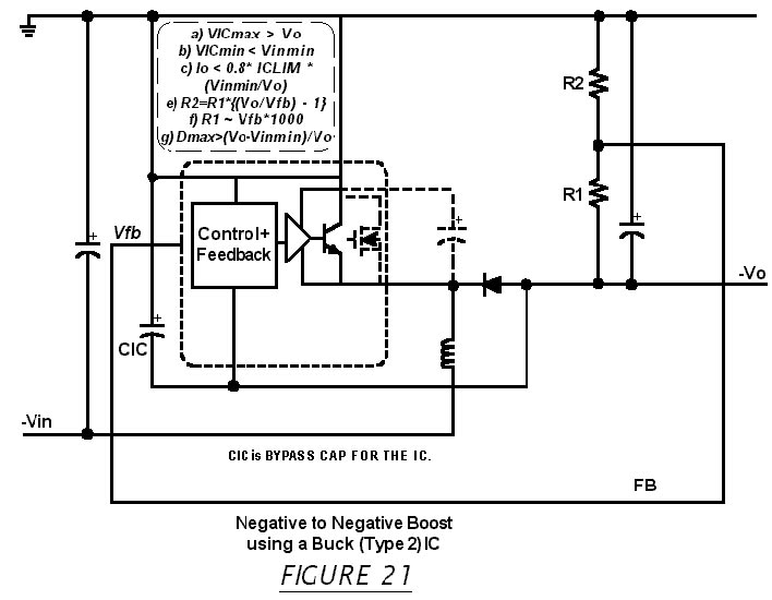
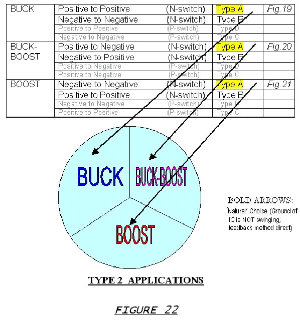
Table 3: With Inductor


Table 4: With Transformer

Note: By convention, R2 is always connected to the higher voltage rail of output and R1 to the lower. * Type 1 IC is a 'Boost/Buck-Boost/Flyback IC'. Type 2 IC is a 'Buck IC'. ** For Figure 11 and 12, more accurate differential amplifier sensing can be used: see Table 3. *** Vfb is NOT the voltage on feedback pin of IC in Figure 17. Also, set zener voltage Vz significantly higher than Vr (typically 20-30% higher) to minimize losses in zener and to maximize efficiency.
Differential Voltage Sensing
Returning to some of the issues in Part 1 of this article, in Figure 11 and Figure 12, a crude voltage dependent current source was used for output regulation. As mentioned, a more accurate sensing scheme for better output regulation can be implemented by using an op-amp (like the LM324). There are two ways of setting up such a differential amplifier. They are shown in Figure 23 and Figure 24. They are respectively alternatives to Figure 11 (negative to positive Buck-Boost using Type 1 IC), and Figure 12 (negative to negative Buck using Type 1 IC). Note that the inputs to the op-amp are labeled Vo_hi and Vo_lo.
This means that irrespective of how the schematic actually labels them, i.e., which is Vo (or --Vo) and which is ground, these nodes must connect to the upper and lower output rails respectively. Some of the relevant aspects of op-amps must be kept in mind. For example, note that an op-amp has a specified input voltage common mode range. For the LM324 series this number is specified to be 1.5V below the upper supply rail and this parameter is hereby called v' in this article. We require that the voltage on both the input pins of the op-amp stay within this allowed range, or the op-amp cannot be considered fully functional. Since the voltages on these pins are fixed by virtue of the resistors, if the resistors are considered fixed, the only way is to ensure that the common-mode condition is met is to set the op-amp supply rail Vaux+ sufficiently higher. This limit equation is therefore also provided in Table 4. Note that if the required minimum Vaux+ value, is still low enough, it may be possible to connect it to an available DC rail. If not, an additional external rail will need to be created to run the op-amp stage.
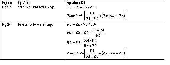
Figure 24 provides much higher gain (if required) and is suited for very low output voltages. If Figure 23 does not work, Figure 24 can be tried for more flexibility. The relevant equations are summarized in Table 5.
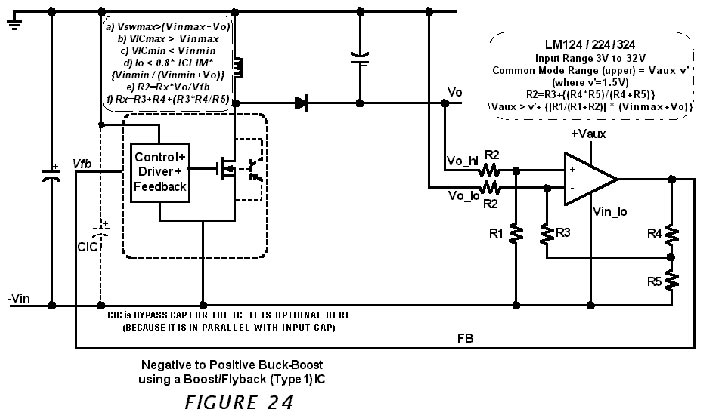
Table 5: Op amp choices
Some Practical Cases
We now present some typical examples to clarify the procedure further.
Example1: The LM2585 is a '3A Flyback regulator'. The datasheet is available at http://www.national.com/ds/LM/LM2585.pdf for more details.
The MIN value of its internal current limit (see its Table of Electrical characteristics) is 3A. Its input operating voltage range is 4V to 40V. Its switch can withstand 65V. Can it be used in a Boost topology? And for what applications?
The following steps are required in this analysis.
1. We identify that the LM2585 is a Type 1 IC by our nomenclature.
2. Referring to the summary chart for Type 1 in Figure 18 (Part 1 of this article), we see that it can be used as say a positive to positive Boost. The corresponding figure is Figure 10 (in Part 1 of this article).
3. Now we consult Figure 10 (Part 1 of this article). This is the required schematic. The feedback scheme is noted. For more detailed design equations for this topology one can refer to the design table under 'Boost' in AN-1246 at http://power.national.com.
4. The relevant selection criteria for suitability are in Table 4. We read off the equations corresponding to Figure 10 in this table and we get the following checklist
5. We see that the input voltage must be below 40V and the output voltage must be below 65V (since Vswmax > Vo and VICmax > Vinmax). These define the input/output voltage conditions for any suitable application.
6. The maximum load current is
So if the output is set to 60V and the input ranges from say 20V to 40V, the maximum load (with a suitably designed practical inductor) is

Example2: The required application conditions are Vin ranging from 4.5V to 5.5V. The output requirement is --5V at 0.5A. Can the LM2651 be used?
LM2651 is a '1.5A Buck Regulator'. Note firstly that this IC can deliver 1.5A in a Buck configuration, but not so in any other configuration/topology. The load rating must then be re-calculated. The following steps are performed.
. 1. We identify the LM2651 as a Type 2 IC according to our nomenclature
2. We refer to Figure 22, which summarizes all the applications of Type 2 ICs. We can see that a positive to negative Buck-Boost is possible with this IC.
3. The relevant schematic is stated to be Figure 20 which we consult for the schematic and feedback scheme.
4. Referring to Table 4 for the selection criteria corresponding to Figure 20:

5. Referring to the datasheet of this device athttp://www.national.com/ds/LM/LM2651.pdf
VICmin=4V
VICmax=14V
ICLIM=1.55A
6. Therefore we now check sequentially for these conditions: a) VICmax>Vinmax+Vo 14V>5.5V+5V=10.5V OK
b) VICmin< 4.5v="" ok="">
c) Io< 0.8*iclim*="" (vinmin/(vinmin+vo)="">< 0.8*1.55*{4.5/(4.5+5)}="0.587" ok="">
The maximum duty cycle can be as low as 92%. Checking for this too: d) Dmax>Vo/(Vo+Vinmin) 0.92>5/(5+4.5)=0.53 OK
Therefore the LM2651 is acceptable for the intended application.
Other Concerns in Topology jumping
One of the main concerns when we jump topologies has to do with a nuance of the topologies themselves. In particular, we must remember that a Buck topology has no Right Half Plane ('RHP') zero, but the Boost and the Flyback/Buck-Boost do. Therefore when we try to take a Buck IC (with internal fixed compensation), we may not have the ability to tailor the crossover frequency to less than 1/4th of the RHP zero frequency as is generally recommended for avoiding this particular mode of instability. So how do we successfully take a Type 2 IC and apply it to other topologies?
To answer that we first must remember the 'intuitive explanation' behind the RHP zero. This is said to occur as follows. If we suddenly increase the load on the output of a Boost or Buck-Boost regulator the output dips momentarily. The voltage on the feedback pin therefore falls slightly and this commands the duty cycle to increase to try and correct for this. But both the Boost and the Buck-Boost are different from the Buck in that during the switch ON-time, NO energy flows into the output...we are basically just building up energy in the inductor during that time. So if the duty cycle increases in response to the load increase, in fact there is a smaller OFF-time, and therefore less rather than more current flows into the output. This causes the output to decrease further. Eventually, after a few cycles, the average inductor current does ramp up progressively and the output dip gets corrected. But before that happens, we can see a situation where the load disturbance is reinforcing itself. In severe cases this may lead to sustained oscillations.
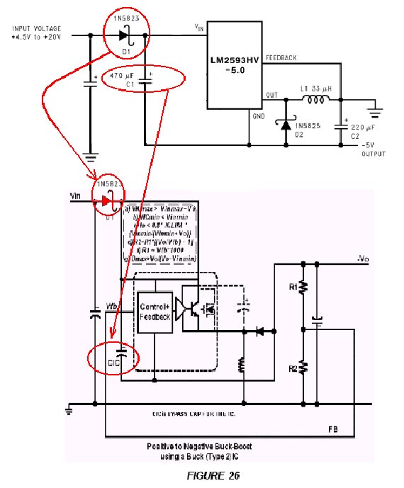
Two well-known RHP zero suppression techniques are used when using a Buck IC to generate other topologies. We show them as applied to a positive to negative configuration. One is shown in Figure 25. This sense when the duty cycle increases suddenly and it thereby pushes up the feedback pin slightly so that it doesn't dip too low in response to the sudden load demand. In Figure 26, we have a typical application circuit as reproduced from the datasheet of LM2593HV, (at http://www.national.com/ds/LM/LM2593HV.pdf ) and we compare the additional components introduced with the schematic in Figure 20. Basically a diode has been inserted and the IC bypass cap is sized to be much bigger now. It is no wonder that the schematic looks much closer to a Buck rather than a Buck-Boost. And in fact during a load transient it does behave temporarily as a Buck, because now significant energy can be transferred from CIC to the output during the switch ON-time. This suppresses the RHP zero significantly, though as compared to Figure 25 it does introduce additional losses across the input diode.
References
a) Application Note AN-1197 at http://power.national.com b) Application Note AN-1246 at http://power.national.com
Acknowledgements
Thanks a lot to the constant encouragement from Mike He to get me to write this and then helping get it published. And my good friends Anand and Vandana Gupta in making the process enjoyable over the weekends.
转载于:https://www.cnblogs.com/shangdawei/p/4132415.html
最后
以上就是现实饼干最近收集整理的关于It's a Buck; It's a Boost, No! It's a Switcher!的全部内容,更多相关It's内容请搜索靠谱客的其他文章。


发表评论 取消回复