前言:直接开讲,请耐心看完 :
首先,OPM模式的波形可以通过主从模式进行触发,其次,OPM模式的波形本身可以进行波形定制。
1 OPM定义和功能说明
One-pulse mode (OPM) is a particular case of the previous modes. It allows the counter to be started in response to a stimulus and to generate a pulse with a programmable length after a programmable delay.
OPM 模式是一个比较特殊的模式,该模型的参数包括:可以定制的长度和Delay(相位)的波形
Starting the counter can be controlled through the slave mode controller. Generating the waveform can be done in output compare mode or PWM mode.
定时器的触发可以通过主从模式的定时器来控制,而输出波形可以是CC模式或者PWM模式。
Select One-pulse mode by setting the OPM bit in the TIMx_CR1 register. This makes the counter stop automatically at the next update event UEV.
在TIMx_CR1选择OPM模式使能OPM,同时定时器的计数器在下一个Event UEV停止计数
2 OPM设定的定时器通道相关控制寄存器:
2.1 OPM-使能-定时器控制寄存器:
TIM1 and TIM8 control register 1 (TIMx_CR1)

OPM模式,其实就是在一个脉冲波形后暂停计数,就这么简单,后面也方便你定制。
Bit 3 OPM: One pulse mode
0: Counter is not stopped at update event
1: Counter stops counting at the next update event (clearing the bit CEN)
2.2 OPM-波形的设定:
使能OPM之后,后面就是对OPM的输出波形进行设置:波形的设定,用CC(捕捉比较)的方式, 就是用定时器的计数去比较你的各种设定,然后,各种翻转逻辑,最后实现波形的定制。
A pulse can be correctly generated only if the compare value is different from the counter initial value.
后面要做的事情就是CNT(counter的计数)和CCRx ARR进行比较,当然在比较之前,如下:
Before starting (when the timer is waiting for the trigger), the configuration must be:
(向上计数的时候)CNT的计数应该小于CCRX或 ARR这样才能产生波形。
• In upcounting: CNT < CCRx ≤ ARR (in particular, 0 < CCRx)
• In downcounting: CNT > CCRx
2.2.1 设定输出波形的细节
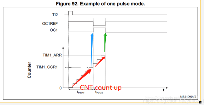
The OPM waveform is defined by writing the compare registers (taking into account the clock frequency and the counter prescaler).
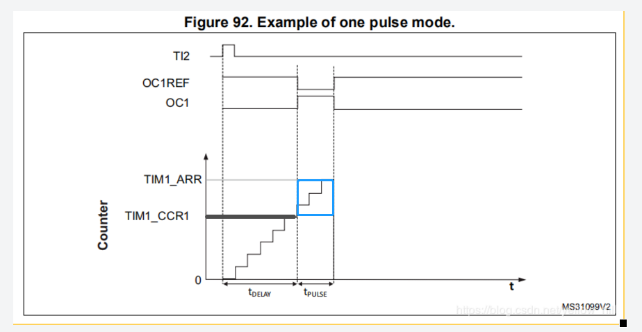
• The tDELAY is defined by the value written in the TIMx_CCR1 register.
我们知道CCR为CC模式的比较值,这个值来决定Delay也就是相位
• The tPULSE is defined by the difference between the auto-reload value and the compare value (TIMx_ARR - TIMx_CCR1).
自动装载值和比较值之间的差值用了决定脉宽
• Let us say the user wants to build a waveform with a transition from ‘0’ to ‘1’ when a compare match occurs and a transition from ‘1’ to ‘0’ when the counter reaches the auto-reload value.
我们假设我们的波形在CC模式比较匹配时候为高电平翻转,而当定时器计数达到自动装载值的时候为低电平翻转。所谓CC模式比较匹配,就是CNT = CCRx,这时候电平翻转到高,定时器计数达到自动装载值,就是CNT = ARR的时候,高电平变成低电平下图做了一些修改,原图遗失CCR1的横坐标线
对于输出的波形有多种选择,
To do this, enable PWM mode 2 by writing OC1M=111 in the TIMx_CCMR1 register.
111: PWM mode 2 - In upcounting, channel 1 is inactive as long as TIMx_CNT<TIMx_CCR1
else active. In downcounting, channel 1 is active as long as TIMx_CNT>TIMx_CCR1 else
inactive.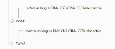
The user can optionally enable the preload registers by writing OC1PE=’1’ in the TIMx_CCMR1 register and ARPE in the TIMx_CR1 register.
Bit 3 OC1PE: Output Compare 1 preload enable
0: Preload register on TIMx_CCR1 disabled. TIMx_CCR1 can be written at anytime, the
new value is taken in account immediately.
1: Preload register on TIMx_CCR1 enabled. Read/Write operations access the preload
register. TIMx_CCR1 preload value is loaded in the active register at each update event.
Bit 7 ARPE: Auto-reload preload enable
0: TIMx_ARR register is not buffered
1: TIMx_ARR register is buffered
In this case the compare value must be written in the TIMx_CCR1 register, the auto-reload value in the TIMx_ARR register, generate an update by setting the UG bit and wait for external trigger event on TI2.
(STM32手册这里好像有错误,应该是CC2P,不是CC1P)CC2P is written to ‘0’ in this example.
In our example, the DIR and CMS bits in the TIMx_CR1 register should be low.
Bits 6:5 CMS[1:0]: Center-aligned mode selection 00: Edge-aligned mode. The counter counts up or down depending on the direction bit (DIR).
Bit 4 DIR: Direction 0: Counter used as upcounter
The user only wants one pulse (Single mode), so '1’ must be written in the OPM bit in the TIMx_CR1 register to stop the counter at the next update event (when the counter rolls over from the auto-reload value back to 0). When OPM bit in the TIMx_CR1 register is set to '0', so the Repetitive Mode is selected. Particular case: OCx fast enable:
OPM模式也可以转成多波复制的模式,只需要OPM 位设为0即可。
In One-pulse mode, the edge detection on TIx input set the CEN bit which enables the counter. Then the comparison between the counter and the compare value makes the output toggle. But several clock cycles are needed for these operations and it limits the minimum delay tDELAY min we can get.
局限性:就是Delay的最小时间是系统局限的,因为上述信号接入需要一点时间:
If the user wants to output a waveform with the minimum delay, the OCxFE bit in the TIMx_CCMRx register must be set. Then OCxRef (and OCx) are forced in response to the stimulus, without taking in account the comparison. Its new level is the same as if a compare match had occurred. OCxFE acts only if the channel is configured in PWM1 or PWM2 mode.
注意:
要立即响应的得到最小Delay的话,需要使能OCXFE位,改位用来强制OCx对OCXREF的响应加速。
这个代价换来的意义是,多了仅仅两个时钟周期的响应时间。


For example the user may want to generate a positive pulse on OC1 (输出比较)with a length of tPULSE and after a delay of tDELAY as soon as a positive edge is detected on the TI2 input pin.
2.3 设置触发和时钟通道,定时器信号通道选择:
-
Let’s use TI2FP2 as trigger 1:
选择触发信号:下图为Timer channel的图

我们这样理解定时器通道,定时器通道分成两个部分:输入、输出
输入的部分我们看:
TI1 、TI2这些都是input,输入通道包括输入滤波(可以滤除小的脉冲)和边沿检测,这样就到了TIxFPx(也就是输入经过滤波和预分频检测后的波形,叫做TI2FP2 Filtered Timer2 Input 2)。然后是,
IC1,input capture输入捕捉通道,也属于输入吧,这里又有在预分频后的信号叫,ICx,(每个信号给他定一个名称就是为了后面负责的通道组合做好标识)。然后是,
OC,输出比较通道,现在开始算输出通道。在进入输出通道OC之前,要开始做复杂的波形运算,达到我们想要的波形。就必须通过捕捉比较寄存器。通过设定通道的OCXREF、DTG的给到输出通道。
• Map TI2FP2 to TI2 by writing CC2S=’01’ in the TIMx_CCMR1 register.
将定时器输入通道TI2连接到TI2FP2,实际上是启用了CH2,
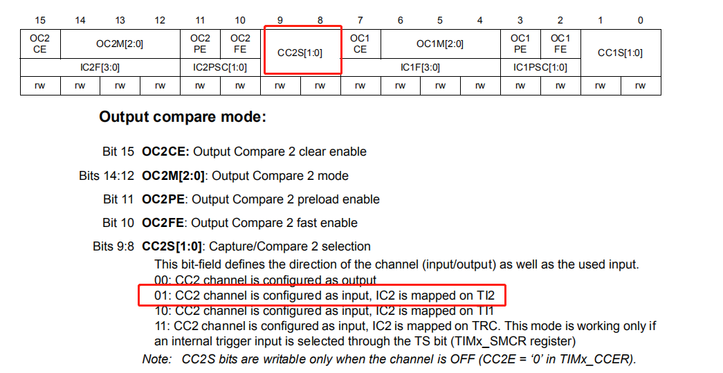
将

通道设定之后,通道的输出也就设定好了。
• TI2FP2 must detect a rising edge, write CC2P=’0’ in the TIMx_CCER register.

Bit 1 CC1P: Capture/Compare 1 output polarity
CC1 channel configured as output:
0: OC1 active high
1: OC1 active low
• Configure TI2FP2 as trigger for the slave mode controller (TRGI) by writing TS=’110’ in the TIMx_SMCR register.
准备将TI2FP2作为从控制器的输入:

TIM1 and TIM8 slave mode control register (TIMx_SMCR)
Bits 6:4 TS[2:0]: Trigger selection
This bit-field selects the trigger input to be used to synchronize the counter.
000: Internal Trigger 0 (ITR0)
001: Internal Trigger 1 (ITR1)
010: Internal Trigger 2 (ITR2)
011: Internal Trigger 3 (ITR3)
100: TI1 Edge Detector (TI1F_ED)
101: Filtered Timer Input 1 (TI1FP1)
110: Filtered Timer Input 2 (TI2FP2)
111: External Trigger input (ETRF)
• TI2FP2 is used to start the counter by writing SMS to ‘110’ in the TIMx_SMCR register (trigger mode).
Bits 2:0 SMS: Slave mode selection
When external signals are selected the active edge of the trigger signal (TRGI) is linked to the polarity selected on the external input (see Input Control register and Control Register description.
000: Slave mode disabled - if CEN = ‘1’ then the prescaler is clocked directly by the internal clock.
001: Encoder mode 1 - Counter counts up/down on TI2FP1 edge depending on TI1FP2 level.
010: Encoder mode 2 - Counter counts up/down on TI1FP2 edge depending on TI2FP1 level.
011: Encoder mode 3 - Counter counts up/down on both TI1FP1 and TI2FP2 edges depending on the level of the other input.
100: Reset Mode - Rising edge of the selected trigger input (TRGI) reinitializes the counter and generates an update of the registers.
101: Gated Mode - The counter clock is enabled when the trigger input (TRGI) is high. The counter stops (but is not reset) as soon as the trigger becomes low. Both start and stop of the counter are controlled.
110: Trigger Mode - The counter starts at a rising edge of the trigger TRGI (but it is not reset). Only the start of the counter is controlled.
111: External Clock Mode 1 - Rising edges of the selected trigger (TRGI) clock the counter.
最后,来一个重点中的重点,相位调节示意图:
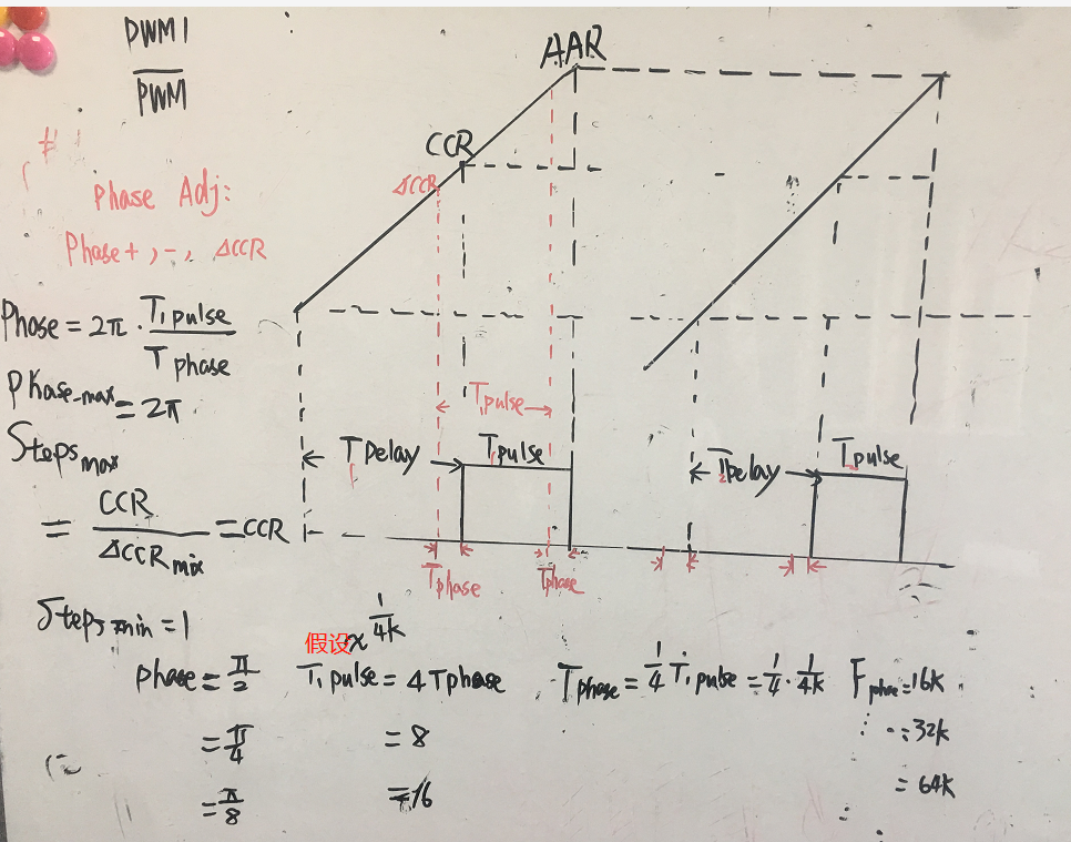
最后
以上就是甜蜜大神最近收集整理的关于STM32 - 定时器的设定 -高级- 08 - One-pulse mode - 触发波的实现 - 可变长度和相位1 OPM定义和功能说明2 OPM设定的定时器通道相关控制寄存器:的全部内容,更多相关STM32内容请搜索靠谱客的其他文章。


发表评论 取消回复