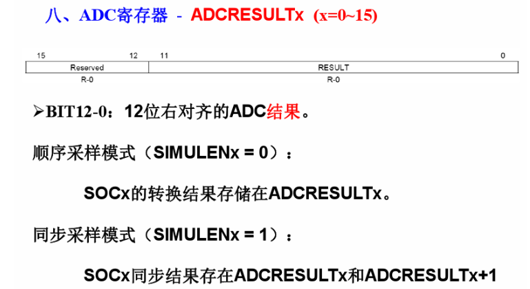
adc简介
SOC
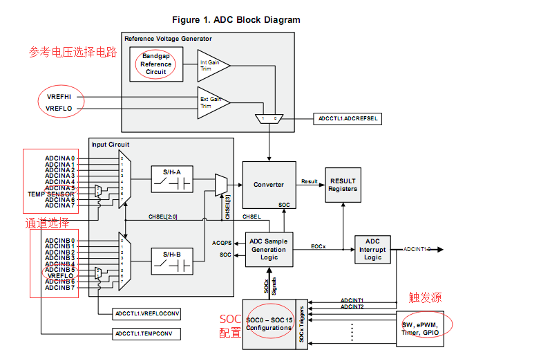
TMS320F28027的ADC为3型,是基于SOC的而不是基于序列的。SOC是一种配置设置,它定义的是单通道单转换。包含3个配置:启动转换的触发源、转换通道、采样保持窗口。每个SOC都是单独配置,即触发源、通道、采样保持窗口可任意组合,可实现从“使用不同触发器、不同通道的单独采样”到“使用单个触发器、相同通道的过采样”。
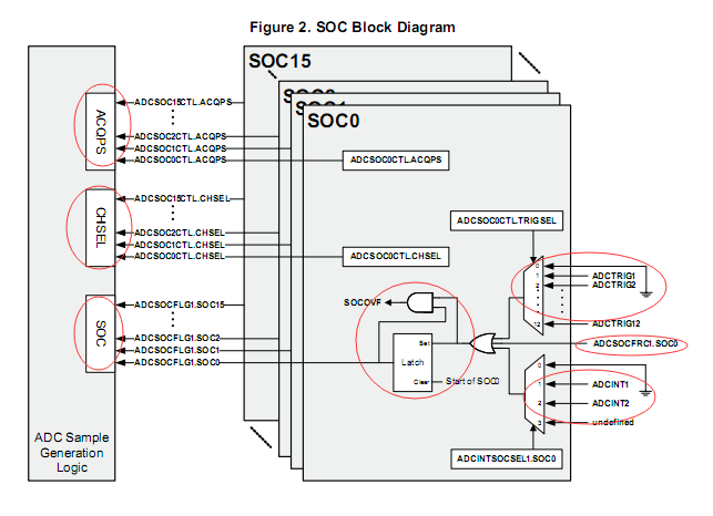
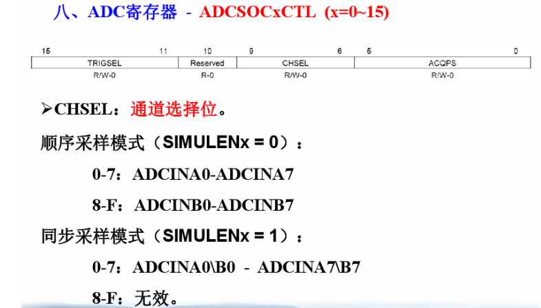
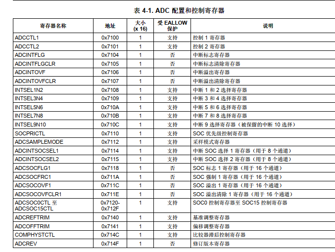
- ADCSOCxCTL: SOCx控制寄存器 (x =0~15)
- ADCSOCFLG: SOC标志寄存器
触发源 4个
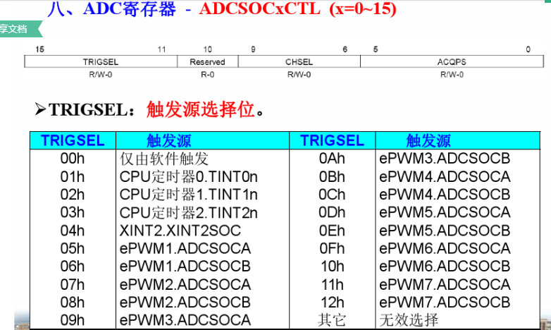
通道 A/B 8个
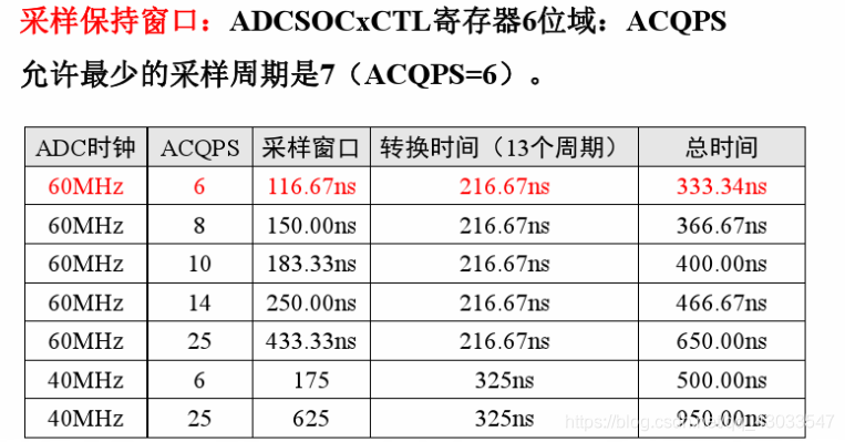
采样保持窗口:
**外部驱动能力的不同影响推动模拟信号速度和有效性。有一些电路需要更长的时间,使电荷正确地转移到ADC的采样电容。为了满足需求,ADC可以在SOC中独立地控制采样窗口的宽度。每个ADCSOCxCTL寄存器都有6位域,ACQPS,用来决定采样保持窗口的大小。写到这个位域的值要比期望的采样保持窗口的包括的周期要少1。例如:位域的值为15,那就需要16个周期来采样。允许最少的采样周期是7(ACQPS=6)。完成一次转换的时间由采样时间加转换时间(13个ADC时钟)组成**
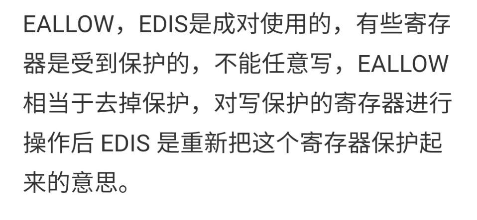
受EALLOW保护
adc的连接
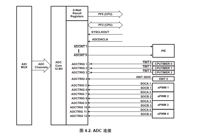
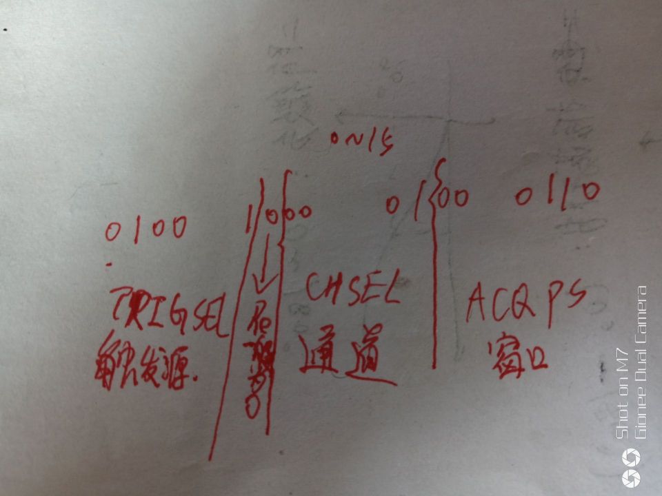
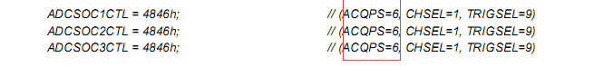
例如,要确保通道ADCINA1上的单个转换在ePWM3计时器达到其周期匹配时发生,必须首先设置ePWM3,以便在周期匹配上输出SOCA或SOCB信号。参见TMS320x2802x Piccolo增强脉冲宽度调制器模块用户指南(SPRUGE9),了解如何做到这一点。在本例中,我们将使用SOCA。然后,使用它的ADCSOCxCTL寄存器设置SOC中的一个。我们选择哪个soc无关紧要,所以我们将使用SOCO。ADC最快的采样窗口为7个循环。为示例窗口选择最快的时间,通道ADCINA1用于通道转换,ePWM3用于SOCO触发器,我们将设置ACQPS字段到6,CHSEL字段到1和TRIGSEL字段到9。写入寄存器的结果值为:
当这样配置时,将在ePWM3 SOCA事件上启动一次ADCINA1的转换,其结果值存储在ADCRESULTO寄存器中。如果ADCINA1需要3倍的过采样。可以给soc1 soc2 SoC3赋予与SOco相同的构型
外部驱动程序能够快速有效地驱动模拟信号。有些电路需要更长的时间才能正确地将电荷转移到ADC的采样电容中。为了解决这个问题,ADC支持控制样本窗口长度为每个单独的SOC实现方式。每个ADCSOCxCTL reaister都有一个6位字段ACQPS。这决定了采样和保持(S/H)窗口大小写入该字段的值比该SOC的采样窗口所需的周期数少一个。因此,该字段中的值15将给出16个时钟周期的采样时间。允许的最小采样周期数为7 (ACQPS-6)。总采样时间是通过将采样窗口大小添加到ADC的转换时间中得到的。13 ADC的时钟。

ADC编程步骤
初始化程序 123固定
void InitAdc(void)
{
    extern void DSP28x_usDelay(Uint32 Count);

    // *IMPORTANT*
    // The Device_cal function, which copies the ADC calibration values from TI reserved
    // OTP into the ADCREFSEL and ADCOFFTRIM registers, occurs automatically in the
    // Boot ROM. If the boot ROM code is bypassed during the debug process, the
    // following function MUST be called for the ADC to function according
    // to specification. The clocks to the ADC MUST be enabled before calling this
    // function.
    // See the device data manual and/or the ADC Reference
    // Manual for more information.

        EALLOW;
        SysCtrlRegs.PCLKCR0.bit.ADCENCLK = 1;//使能ADC模块时钟
        (*Device_cal)();
        EDIS;

    // To powerup the ADC the ADCENCLK bit should be set first to enable
    // clocks, followed by powering up the bandgap, reference circuitry, and ADC core.
    // Before the first conversion is performed a 5ms delay must be observed
    // after power up to give all analog circuits time to power up and settle

    // Please note that for the delay function below to operate correctly the
    // CPU_RATE define statement in the DSP2802x_Examples.h file must
    // contain the correct CPU clock period in nanoseconds.
    EALLOW;
    AdcRegs.ADCCTL1.bit.ADCBGPWD  = 1;      // Power ADC BG  带隙
    AdcRegs.ADCCTL1.bit.ADCREFPWD = 1;      // Power reference 参考源
    AdcRegs.ADCCTL1.bit.ADCPWDN   = 1;      // Power ADC 启动模拟电路
    AdcRegs.ADCCTL1.bit.ADCENABLE = 1;      // Enable ADC  使能ADC
    AdcRegs.ADCCTL1.bit.ADCREFSEL = 0;      // Select interal BG 选择内部带隙
    EDIS;

    DELAY_US(ADC_usDELAY);         // Delay before converting ADC channels
}
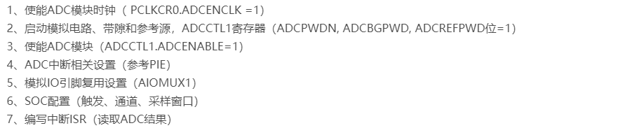
初始化函数已经把我们的前三步都做完了,也就是使能时钟、上电、使能ADC模块;

那我们现在来进行SOC相关设置,也就是:触发源、采样时隙、通道选择。
*触发源*我们选择定时器0,因为我们做测试肯定输入一个稳定的直流电压,那用定时器最方便。
AdcRegs.ADCSOC0CTL.bit.TRIGSEL = 1;

采样时隙就用最短时隙,也就是AdcRegs.ADCSOC0CTL.bit.ACQPS = 6;
由于TI那个实验板只引出了几个ADC引脚而已,我们就用ADCINA1,也就是 AdcRegs.ADCSOC0CTL.bit.CHSEL = 1;
另外,我们说了,我们本次的实验是顺序采样,迟中断,那就是:
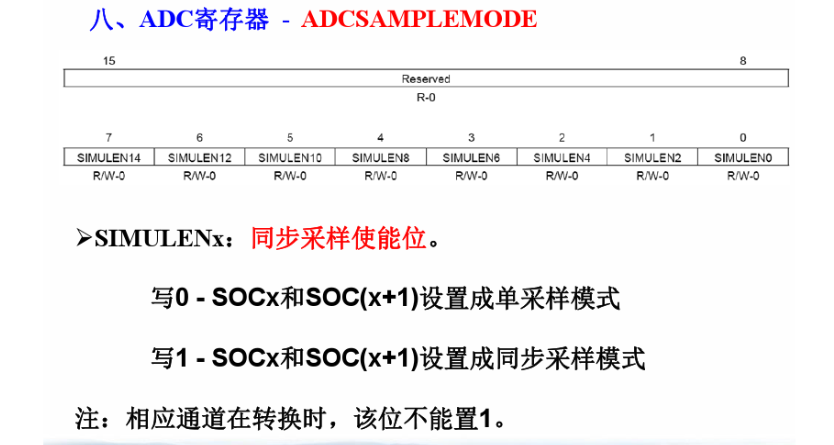
AdcRegs.ADCSAMPLEMODE.bit.SIMULEN0 = 1;
AdcRegs.ADCCTL1.bit.INTPULSEPOS = 1;
到这里SOC相关设置就完成了
 AdcRegs.ADCSOC0CTL.bit.CHSEL         = 1;        //set SOC0 channel select to ADCINA0              选择AD通道  1
 AdcRegs.ADCSOC0CTL.bit.TRIGSEL         = 1;        //set SOC0 start trigger on timer 0 only          选择AD触发方式
 AdcRegs.ADCSOC0CTL.bit.ACQPS         = 6;        //set SOC0 S/H Window to 7 ADC Clock Cycles, (6 ACQPS plus 1)  配置转换时间
 AdcRegs.ADCSAMPLEMODE.bit.SIMULEN0 = 1;  //顺序采样
 AdcRegs.ADCCTL1.bit.INTPULSEPOS = 1;
 EDIS;
最后还要再PIE组里面打开ADCINT1开关:PieCtrlRegs.PIEIER1.bit.INTx1 = 1;
ADC中断函数就一个置位:
interrupt void ADCINT1_ISR(void)   // ADC  (Can also be ISR for INT10.1 when enabled)
{
  // Insert ISR Code here

  // To receive more interrupts from this PIE group, acknowledge this interrupt
   PieCtrlRegs.PIEACK.all = PIEACK_GROUP1;

  // Next two lines for debug only to halt the processor here
  // Remove after inserting ISR Code

  //asm ("      ESTOP0");
  //for(;;);

}
定时器
void InitCpuTimers(void)
{
    // CPU Timer 0
    // Initialize address pointers to respective timer registers:
    CpuTimer0.RegsAddr = &CpuTimer0Regs;
    // Initialize timer period to maximum:
    CpuTimer0Regs.PRD.all  = 1000;
    // Initialize pre-scale counter to divide by 1 (SYSCLKOUT):
    CpuTimer0Regs.TPR.bit.TDDR  = 59;
    CpuTimer0Regs.TPRH.bit.TDDRH = 0;
    // Make sure timer is stopped:
    CpuTimer0Regs.TCR.bit.TSS = 1;
    // Reload all counter register with period value:
    CpuTimer0Regs.TCR.bit.TRB = 1;
    // Reset interrupt counters:
    CpuTimer0.InterruptCount = 0;

// CpuTimer 1 and CpuTimer2 are reserved for DSP BIOS & other RTOS
// Do not use these two timers if you ever plan on integrating
// DSP-BIOS or another realtime OS.
//
// Initialize address pointers to respective timer registers:
    CpuTimer1.RegsAddr = &CpuTimer1Regs;
    CpuTimer2.RegsAddr = &CpuTimer2Regs;
    // Initialize timer period to maximum:
    CpuTimer1Regs.PRD.all  = 0xFFFFFFFF;
    CpuTimer2Regs.PRD.all  = 0xFFFFFFFF;
    // Initialize pre-scale counter to divide by 1 (SYSCLKOUT):
    CpuTimer1Regs.TPR.all  = 0;
    CpuTimer1Regs.TPRH.all = 0;
    CpuTimer2Regs.TPR.all  = 0;
    CpuTimer2Regs.TPRH.all = 0;
    // Make sure timers are stopped:
    CpuTimer1Regs.TCR.bit.TSS = 1;
    CpuTimer2Regs.TCR.bit.TSS = 1;
    // Reload all counter register with period value:
    CpuTimer1Regs.TCR.bit.TRB = 1;
    CpuTimer2Regs.TCR.bit.TRB = 1;
    // Reset interrupt counters:
    CpuTimer1.InterruptCount = 0;
    CpuTimer2.InterruptCount = 0;

}
定时器中断
interrupt void  TINT0_ISR(void)      // CPU-Timer 0
{
  // Insert ISR Code here

  // To receive more interrupts from this PIE group, acknowledge this interrupt
  PieCtrlRegs.PIEACK.all = PIEACK_GROUP1;

  // Next two lines for debug only to halt the processor here
  // Remove after inserting ISR Code
//  asm ("      ESTOP0");
//  for(;;);
}
相关中断设置
   CpuTimer0Regs.TCR.bit.TIE = 1;
   StartCpuTimer0();
   EALLOW;
   PieCtrlRegs.PIEIER1.bit.INTx7 = 1;
   PieCtrlRegs.PIECTRL.bit.ENPIE = 1;
   IER |= 0x0001;
   EINT;
   EDIS;
显示
   while(1)
   {
       if(AdcRegs.ADCSOCFLG1.bit.SOC0==1)
       {
           while(AdcRegs.ADCSOCFLG1.bit.SOC0==1);
           AdcRegs.ADCINTFLGCLR.bit.ADCINT1 = 1;
           DELAY_US(10);
           sum+=AdcResult.ADCRESULT0;
           i++;
       }
       if(i==100)
       {
           sum/=100;
           vol=sum*3.3/4095;
           WRITECMD_LCD12864(0x01);
           DISLPLAY_LONGSTRING(2,0,sum);
           DISLPLAY_FLOATSTRING(3,0,vol);
           WRITEDATA_LCD12864('v');
           sum=0;
           i=0;
       }
   }
主要参考:https://blog.csdn.net/BHK_SOFTWARE/article/details/52137577
寄存器讲解 https://wenku.baidu.com/view/e14aaf55d15abe23492f4d52.html?pn=51
程序代码 https://blog.csdn.net/w471176877/article/details/8049697
http://bbs.eeworld.com.cn/thread-475877-1-1.html
	 主频:60M
     描述:练习ADC,同时采样模式,ADCINA4与ADCINB4
     CPU TIM0为触发,同时采样两路电压
#include "DSP28x_Project.h"     // Device Headerfile and Examples Include File
#include "LEDs.h"

interrupt void tim0_isr(void);
interrupt void ADC_convered(void);

Uint16 ADCINA4_Voltage_sum = 0;
Uint16 ADCINB4_Voltage_sum = 0;
Uint16 ADCINA4_Voltage = 0;
Uint16 ADCINB4_Voltage = 0;
char convered_count = 0;

void main(void)
{

// Step 1. Initialize System Control:
// PLL, WatchDog, enable Peripheral Clocks
// This example function is found in the DSP2802x_SysCtrl.c file.
   InitSysCtrl();

// Step 2. Initalize GPIO:
// This example function is found in the DSP2802x_Gpio.c file and
// illustrates how to set the GPIO to it's default state.
// InitGpio();  // Skipped for this example


// Step 3. Clear all interrupts and initialize PIE vector table:
// Disable CPU interrupts
   DINT;

// Initialize PIE control registers to their default state.
// The default state is all PIE interrupts disabled and flags
// are cleared.
// This function is found in the DSP2802x_PieCtrl.c file.
   InitPieCtrl();

// Disable CPU interrupts and clear all CPU interrupt flags:
   IER = 0x0000;
   IFR = 0x0000;

// Initialize the PIE vector table with pointers to the shell Interrupt
// Service Routines (ISR).
// This will populate the entire table, even if the interrupt
// is not used in this example.  This is useful for debug purposes.
// The shell ISR routines are found in DSP2802x_DefaultIsr.c.
// This function is found in DSP2802x_PieVect.c.
   InitPieVectTable();


// Step 4. Initialize all the Device Peripherals:
// This function is found in DSP2802x_InitPeripherals.c
// InitPeripherals(); // Not required for this example

// Step 5. User specific code:

   InitAdc();

   EALLOW;

   AdcRegs.ADCSAMPLEMODE.bit.SIMULEN0 = 1; //同时采样
   AdcRegs.ADCSOC0CTL.bit.CHSEL = 4;       //soc通道选择
   AdcRegs.ADCSOC1CTL.bit.CHSEL = 12;
   AdcRegs.ADCSOC0CTL.bit.ACQPS = 6;     //采样时间
   AdcRegs.ADCSOC1CTL.bit.ACQPS = 6;
   AdcRegs.ADCSOC0CTL.bit.TRIGSEL = 1;    //soc触发选择,TIM0
   AdcRegs.ADCCTL1.bit.INTPULSEPOS	= 1;  //结果存入寄存器才产生中断

   PieVectTable.ADCINT1 = &ADC_convered;
   AdcRegs.INTSEL1N2.bit.INT1SEL = 1;    //中断线1选择soc1
   AdcRegs.INTSEL1N2.bit.INT1CONT  = 0;
   AdcRegs.INTSEL1N2.bit.INT1E	= 1;	//中断使能

   PieCtrlRegs.PIEIER1.bit.INTx1 = 1;	//使能int1.1
   EDIS;

/****************设置定时器,用以触发ADC*****************/
   CpuTimer0Regs.TPR.bit.TDDR = 59;
   CpuTimer0Regs.TPRH.bit.TDDRH = 0; //对输入时钟60分频,60M/60=1M
   CpuTimer0Regs.PRD.all = 500000;//定时0.5s
   CpuTimer0Regs.TCR.bit.TRB = 1; //reload
   CpuTimer0Regs.TCR.bit.TIE = 1; //使能中断
   CpuTimer0Regs.TCR.bit.TSS = 0; //开始计数

   EALLOW;
   PieVectTable.TINT0 = &tim0_isr;
   PieCtrlRegs.PIECTRL.bit.ENPIE = 1;	//使能PIE
   PieCtrlRegs.PIEIER1.bit.INTx7 = 1;	//使能int1.7
   IER |= 0x0001;//使能GROUP1
   EINT;
   EDIS;

   LEDs_init();
   while(1)
   {
   };
}

interrupt void ADC_convered(void)
{

	LED_toggle(LED2);
	ADCINA4_Voltage_sum += AdcResult.ADCRESULT0;
	ADCINB4_Voltage_sum += AdcResult.ADCRESULT1;
	AdcRegs.ADCINTFLGCLR.bit.ADCINT1 = 1;
	PieCtrlRegs.PIEACK.all = PIEACK_GROUP1;
	convered_count++;
	/*********转换16次,取平均值*********/
	if(convered_count > 15)
	{
		ADCINA4_Voltage = ADCINA4_Voltage_sum >> 4;//相当于除以16
		ADCINB4_Voltage = ADCINB4_Voltage_sum >> 4;
		ADCINA4_Voltage_sum = 0;
		ADCINB4_Voltage_sum = 0;
		convered_count = 0;
	}
}

interrupt void tim0_isr(void)
{
	LED_toggle(LED0);
	PieCtrlRegs.PIEACK.all = PIEACK_GROUP1;
}
---------------------
作者:w471176877
来源:CSDN
原文:https://blog.csdn.net/w471176877/article/details/8049697
版权声明:本文为博主原创文章,转载请附上博文链接!
		配置ADC单通道软件强制转换 ,配合程序来解释ADC配置的思路。
    step 1:
             InitSysCtrl();  // 系统初始化子程序,在DSP28_sysctrl.c中,PLL,关闭看门狗,使能外围模块
    step 2:
              InitPieCtrl();  //初始化PIE控制寄存器,恢复默认设置
              IER = 0x0000;//CPU禁止使能
              IFR = 0x0000;//清楚CPU所有中断标志
              InitPieVectTable();//初始化PIE向量表
    step 3:
              //初始化ADC
            EALLOW;  //使能ADC模块的时钟
            SysCtrlRegs.PCLKCR0.bit.ADCENCLK = 1;
             (*Device_cal)();
             EDIS;
    step 4:
            EALLOW;                            //这部分官方手册建议就按这个顺序配置
            AdcRegs.ADCCTL1.bit.ADCBGPWD  = 1;      // Power ADC BG
            AdcRegs.ADCCTL1.bit.ADCREFPWD = 1;      // Power reference
            AdcRegs.ADCCTL1.bit.ADCPWDN   = 1;      // Power ADC
            AdcRegs.ADCCTL1.bit.ADCENABLE = 1;      // Enable ADC
            AdcRegs.ADCCTL1.bit.ADCREFSEL = 0;      // Select interal BG
           EDIS;
           DELAY_US(ADC_usDELAY);         // Delay before converting ADC channels    step 5:
          EALLOW;          AdcRegs.INTSEL1N2.bit.INT1E     = 1;        //使能    ADCINT1
          //ADCSOCxCTL    x可设置0--15,CHSEL 选择AD输入通道
          AdcRegs.ADCSOC0CTL.bit.CHSEL         = 0;        //set SOC0 channel select to ADCINA0              选择AD通道
          AdcRegs.ADCSOC0CTL.bit.TRIGSEL         = 0;        //set SOC0 start trigger on software only          选择AD触发方式
          AdcRegs.ADCSOC0CTL.bit.ACQPS         = 6;        //set SOC0 S/H Window to 7 ADC Clock Cycles, (6 ACQPS plus 1)  配置转换时间
          EDIS;
   step 6:
           // Enable ADCINT1 in PIE
          PieCtrlRegs.PIEIER1.bit.INTx1 = 1;        // Enable INT 1.1 in the PIE
          IER |= M_INT1;                                                 // Enable CPU Interrupt 1
          EINT;                                                          // Enable Global interrupt INTM
          ERTM;                                                          // Enable Global realtime interrupt DBGM

                for(;;)
                  {
                //Force start of conversion on SOC0
                AdcRegs.ADCSOCFRC1.all = 0x01;
                DELAY_US(1000000);//delay 1s   在死循环里面这样写就可以每1S就会强制ADC转换一次

                  }
         //以下是中断服务函数

interrupt void  adc_isr(void)
{
  Voltage = AdcResult.ADCRESULT0;  //读取AdcResult的值要与自己相对应配置的SOCx相对应,这个程序配置的是SOC0,所以要读取ADCRESULT0。
  vol=Voltage*3.3/4096;
  AdcRegs.ADCINTFLGCLR.bit.ADCINT1 = 1;                //Clear ADCINT1 flag reinitialize for next SOC
  PieCtrlRegs.PIEACK.all = PIEACK_GROUP1;   // Acknowledge interrupt to PIE
  return;
}
最后
以上就是细心月亮最近收集整理的关于f28027 ADC详细学习过程的全部内容,更多相关f28027内容请搜索靠谱客的其他文章。


发表评论 取消回复