学习记录
文章目录
- 学习记录
- 方法一
- 方法二
方法一
自己照着PYNQ-Z1 Board Reference Manual里面的
Memory o 512MB DDR3 with 16-bit bus @ 1050Mbps
5 DDR Memory
The PYNQ-Z1 includes an IS43TR16256A-125KBL DDR3 memory components creating a single rank, 16-bit wide interface and a total of 512MiB of capacity. The DDR3 is connected to the hard memory controller in the Processor Subsystem (PS), as outlined in the Zynq documentation.
The PS incorporates an AXI memory port interface, a DDR controller, the associated PHY, and a dedicated I/O bank.DDR3 memory interface speeds up to 533 MHz/1066 Mbps are supported. (Maximum actual clock frequency is 525 MHz on the PYNQ-Z1 due to PLL limitation.)
PYNQ-Z1 was routed with 40 ohm (+/-10%) trace impedance for single-ended signals, and differential clock and strobes set to 80 ohms (+/-10%). A feature called DCI (Digitally Controlled Impedance) is used to match the drive strength and termination impedance of the PS pins to the trace impedance. On the memory side, each chip calibrates its on-die termination and drive strength using a 240-ohm resistor on the ZQ pin.
Due to layout reasons, the two data byte groups (DQ[0-7], DQ[8-15]) were swapped. To the same effect, the data bits inside byte groups were swapped as well. These changes are transparent to the user. During the whole design process the Xilinx PCB guidelines were followed.
Both the memory chips and the PS DDR bank are powered from the 1.5V supply. The mid-point reference of 0.75V is created with a simple resistor divider and is available to the Zynq as external reference.
For proper operation, it is essential that the PS memory controller is configured properly. Settings range from the actual memory flavor to the board trace delays. For your convenience, the Zynq presets file for the PYNQ-Z1 is provided on the resource center and automatically configures the Zynq Processing System IP core with the correct parameters.
For best DDR3 performance, DRAM training is enabled for write leveling, read gate, and read data eye options in the PS Configuration Tool in Xilinx tools. Training is done dynamically by the controller to account for board delays, process variations and thermal drift. Optimum starting values for the training process are the board delays (propagation delays) for certain memory signals.
Board delays are specified for each of the byte groups. These parameters are board-specific and were calculated from the PCB trace length reports. The DQS to CLK Delay and Board Delay values are calculated specific to the PYNQ-Z1 memory interface PCB design.
For more details on memory controller operation, refer to the Xilinx Zynq Technical Reference manual.
毫无疑问,这是最佳方案,能对ddr有更加深入地理解,缺点是对新手不友好。
方法二
使用官方提供的预设文件。
其实,参考手册也对此进行提示了。
the Zynq presets file for the PYNQ-Z1 is provided on the resource center and automatically configures the Zynq Processing System IP core with the correct parameters.
具体加载方法如下。

-
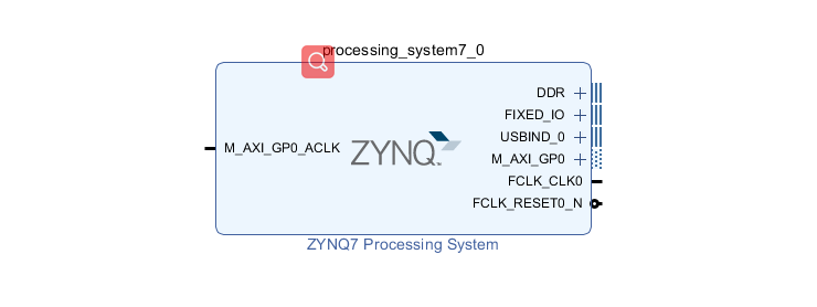
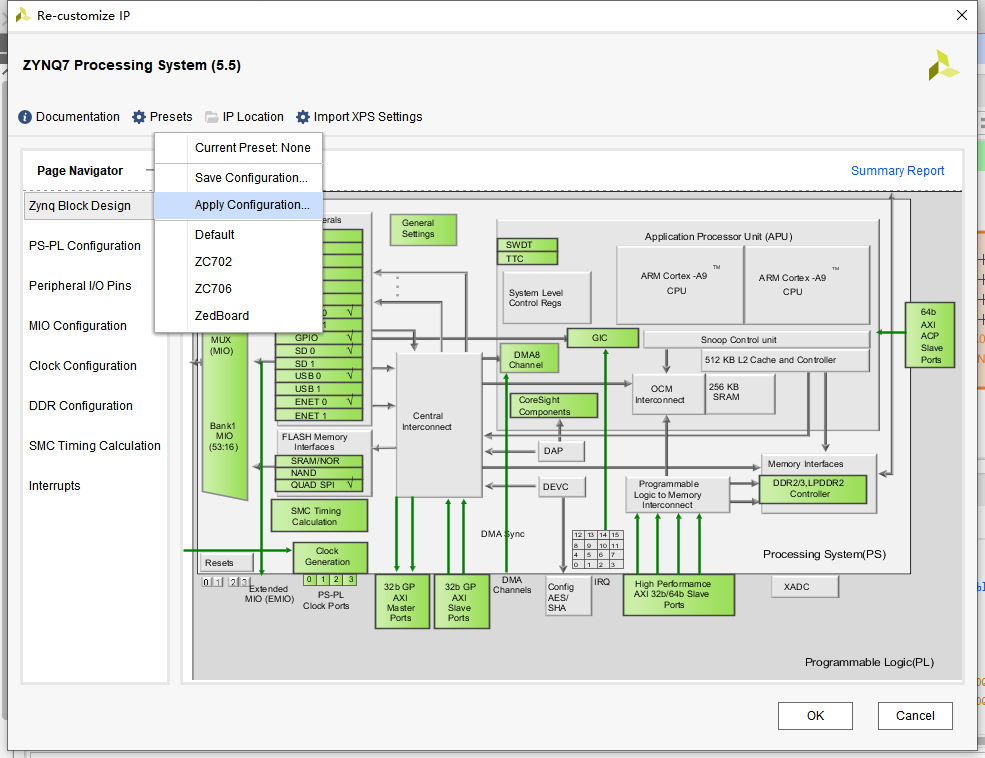
双击IP核

-
左上角点击presets ->apply configuation
-
选择.tcl文件
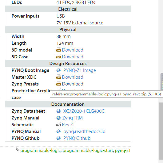
presets文件的下载链接在如下页面
https://reference.digilentinc.com/reference/programmable-logic/pynq-z1/start

文件在页面的左下角。
都看到这了,给文章点个赞再走吧
||
V
最后
以上就是甜蜜香氛最近收集整理的关于PYNQ配置DDR Configuration学习记录的全部内容,更多相关PYNQ配置DDR内容请搜索靠谱客的其他文章。


发表评论 取消回复