Peak Current Mode (PCM)
1 Introduction
The TPS560430 regulator is an easy-to-use synchronous step-down DC/DC converter operating from 4-V to 36-V supply voltage. It is capable of delivering up to 600-mA DC load current in a very small solution size. The family has different versions applicable for different applications, 1.1-MHz and 2.1-MHz switching frequency, PFM and FPWM, adjustable and fixed output voltage. The device is suitable for a wide range of applications from industrial to automotive for power conditioning from an unregulated source. The TPS560430 employs peakcurrent mode control with internal loop compensation, which reduces design time, and requires few external components.
A lot of PCM loop models are available for system design. The most popular model is provided in [2]. The model predicted the sample and hold effects in the current loop, while using a three-terminal switch model to calculate power stage small signal model. Using this method, a simplified loop model is provided in [3], and an equivalent circuit is obtained to simulate the loop response. However, if all of the models require simulation tools to draw the bode plot, then find a crossover frequency and phase margin based on the bode plot. Besides, the transfer function of inner current loop is quite complex, making it hard to understand how it impacts the whole loop response. In this document, a simple equation is provided to calculate bandwidth. The phase margin is obtained by simplifying the inside current loop as a single pole. The inner current loop stability criteria can be obtained based on the model. Each zero and pole in the model has a clear physical meaning, making it easy to analyze the impact of each component value on the loop response. The inductor and output capacitor design procedure of the internally compensated PCM buck converter is given using the model. The model accuracy is verified by both simulation and bench measurement results.
2 Peak Current Mode Loop Modeling
2.1 Overall Control Block Diagram and Transfer Function Derivation
Figure 2-1 shows the simplified schematic for the PCM buck converter.
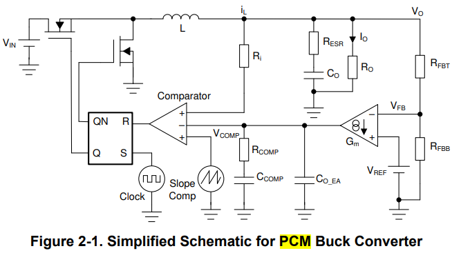
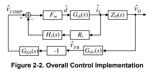
Figure 2-2 shows the overall control block model where:
- • Gdi(s) is the duty cycle to iL transfer function.
- • ZO(s) is the transfer function of output impedance.
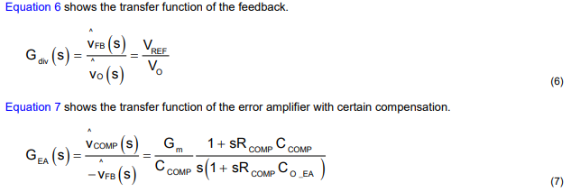
- • Gdiv(s) is the gain of the feedback resistor network.
- • GEA(s) is the transfer function of the error amplifier with certain compensation.
- • Fm is the gain of PCM PWM comparator.
- • Ri is the current sensing resistor.
- • He(s) is the transfer function model of inductor current sampling-hold effect.
Equation 1 shows the transfer function from the inductor current to the output voltage.

Gdi(s) is the duty cycle to iL transfer function.

The internal loop compensation is designed so that the crossover frequency is much higher than the corner frequency, 1/(2π√LCO). For crossover frequency and higher frequency, Equation 2 can be simplified as Equation 3.

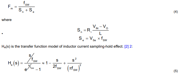
The sensed inductor current, external ramp, and the output of error amplifier VCOMP are compared, which determines when to turn off the high side MOSFET, hence the duty cycle is determined. Fm is the comparator gain. fSW is the switching frequency. Sn is the on-time slope of the sensed-current waveform and Se is the external ramp slope.
2.2 Inside Current Loop Model
Based on Equation 3 to Equation 5 and Figure 2-2, the transfer function from control to inductor current is Gci(s):

For PCM buck converter, the crossover frequency is much smaller than half switching frequency, so around crossover frequency Equation 8 can be simplified as Equation 9. The inside current loop is simplified as a single pole, which is very helpful for the loop response analysis of PCM buck converter.

If the inside current loop Gci(s) is not stable, subharmonic oscillation occurs. A system is stable as long as each of the poles of the closed loop transfer function lies in the left half plane. The minimum inductor value is calculated to prevent subharmonic oscillation:

2.3 Overall Loop Model
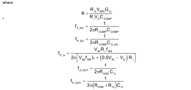
fZ_EA and fP_EA are zeros and poles introduced by the error amplifier with certain compensation. fZ_OUT and fP_OUT are zeros and poles introduced by the output capacitor and load. fP_ci is the pole introduced by the inside current loop. Based on Equation 1, Equation 6, Equation 7, and Equation 9, the open loop transfer function L(s) around crossover frequency is obtained:

2.4 Inductor and Output Capacitor Design Limits
Figure 2-3 shows the Bode plot with proper inductor and output capacitor design. fc ≫ fP_OUT, fc ≫ fZ_EA, fc ≪ fP_EA, fc ≪ fP_ci, fc ≪ fZ_OUT
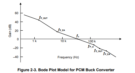
fZ_EA and fP_EA are zeros and poles introduced by the error amplifier with certain compensation.
fZ_OUT and fP_OUT are zeros and poles introduced by the output capacitor and load.
fP_ci is the pole introduced by the inside current loop.
fC is crossover frequency.
The gain curve must go across 0 dB with a -20 dB/dec slew rate, so that the phase margin is enough. The zero introduced by the compensation network fZ_EA cancels the pole of output impedance fP_OUT, and they are placed far before crossover frequency: fP_OUT ≪ fc , fZ_EA ≪ fc . The parasitic capacitor of error amplifier CO_EA is quite small, so fP_EA ≫ fc .
If L is too large, the pole introduced by the current loop fP_ci is smaller than the crossover frequency fc . The gain curve goes across 0 dB with a -40 dB/dec slew rate, and the phase margin is not enough. Besides, the loop response is influenced by VIN since fP_ci is influenced by VIN. To prevent that from happening, L must be properly designed to ensure fP_ci ≫ fc . Equation 12 calculates the maximum inductor value

( ,
, )
)
If the Equivalent Series Resistance (ESR) of output capacitor is too large, the zero introduced by the output capacitor fZ_OUT is smaller than the crossover frequency fc . The gain curve has a 0 dB/dec slew rate after fZ_OUT, which makes the crossover frequency too large. Some high frequency poles introduced by the parasitic parameters in the IC influence the phase margin, and the phase margin is not enough. To prevent that, ESR of the output capacitor must be properly designed to ensure fZ_OUT ≫ fc . Equation 13 calculates the maximum ESR.

2.5 The Equation to Calculate Bandwidth and Phase Margin
From Equation 11 and considering fc ≫ fP_OUT, fc ≫ fZ_EA, fc ≪ fP_EA, fc ≪ fP_ci, and fc ≪ fZ_OUT, the magnitude of open loop transfer function at crossover frequency fc is shown in Equation 14.

Considering RESR ≪ RO, the crossover frequency fc is obtained: Equation 15

Phase margin is the phase of open loop transfer function at fc minus -180°: Equation 16

3 Inductor and Output Capacitor Design
In this section, the inductor and output capacitor is designed in a practical application using TPS560430XF. The loop response is considered during the process. Table 3-1 lists the design specifications.

3.1 Inductor Design Equation
17 calculates the value of the output conductor. KIND is a coefficient that represents the amount of inductor ripple current relative to the maximum output current of the device. A reasonable value of KIND is 0.2 – 0.4. Since the ripple current increases with the input voltage, the maximum input voltage is used to calculate the minimum inductance LMIN, while KIND = 0.4 is selected. The minimum inductor value is calculated to be 16.3 μH. Choose the nearest standard inductor: L= 18 μH.

From Equation 12, the maximum inductor value is calculated to get enough phase margin. Three times margin is suggested and the limit is Equation 18 with the TPS560430 internal parameter. If you assume the target crossing over frequency fc is about 20 kHz, then the result is L < 40 μH at the minimum VIN. The selected 18-μH inductor meets the requirement.

The TPS560430 is protected from over-current conditions by the cycle-by-cycle current limit. To prevent inductor saturation in case of short circuit conditions, the inductor saturation current must be greater than the device maximum peak current limit, which is 1.4 A for the TPS560430.
3.2 Output Capacitor Design
The output capacitor is designed based on output ripple and loop response. The output voltage ripple is composed of two parts. One is caused by the inductor current ripple going through the ESR of the output capacitor, see Equation 19. The other is caused by the inductor current ripple charging and discharging the output capacitor, see Equation 20. The target output ripple is 30 mV, so ΔVO_ESR < 30 mV and ΔVO_C < 30 mV, then RESR < 125 mΩ and CO > 0.91 μF.

From Equation 13, the maximum ESR value is calculated to get a reasonable crossover frequency and enough phase margin. If you assume the target crossing over frequency fc is about 20 kHz, then the result is RESR ≪ 612 mΩ. Three times margin is suggested and the result is RESR < 204 mΩ.
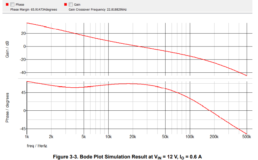
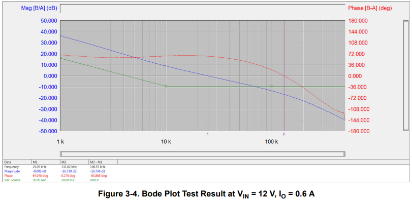
Output capacitor value determines loop response in internally compensated PCM buck converters, as Equation 15 and Equation 16. With TPS560430 internal parameter, the calculation equation is as Equation 21 and Equation 22. The target fc is about 20 kHz, so CO is about 15 μF. Consider of derating, one 22-μF, 16-V ceramic capacitor with 4-mΩ ESR is used. The capacitance after derating is 13 μF: CO = 13 μF, RESR = 4 mΩ. The crossover frequency is fc = 23.4 kHz and the phase margin is calculated as 64.2° at VIN = 12 V, IO = 0.6 A. The equation also indicates that the worst phase margin happens at minimum VIN and minimum IO, while the calculation result is 59.2° at VIN = 7 V, IO = 0.1 A. They meet design specs.

3.3 Simulation and Bench Verification
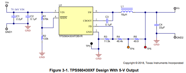
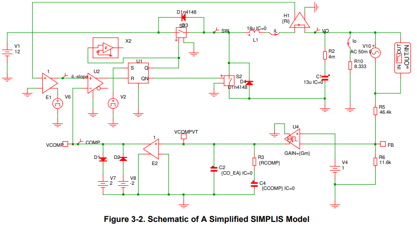
Figure 3-1 shows the schematic for bench verification. SIMPLIS is used to simulate the loop response as shown in Figure 3-2. Figure 3-3 and Figure 3-4 are the loop responses from the SIMPLIS simulation and bench test under VIN = 12 V, VO = 5 V, IO = 0.6 A, and fSW = 1.1 MHz. Table 3-2 compares the calculation results, simulation results, and bench measurement at different VIN. It can be seen that the proposed model in this application report is accurate.

4 Summary
For an internally compensated, peak current mode buck converter, consider the loop response when designing inductor and output capacitor. This application report simplifies the inside current loop as a single pole, provides the constraint to ensure loop stability, and gives out an equation to calculate bandwidth and phase margin. The inductor and output capacitor is designed step-by-step considering loop response. The theory is verified by simulation and bench measurement results.
5 References
- 1. Texas Instruments, TPS560430 4-V to 36-V, 600-mA Synchronous Step-Down Converter Data Sheet
- 2. R.B. Ridley, A New Small-Signal Model for Current-Mode Control, PhD Dissertation, Virginia Polytechnic Institute and State University, November, 1990.
- 3. Texas Instruments, TPS65270 Loop Compensation Design Consideration Application Report
- 4. Texas Instruments, How to Evaluate the Maximum Inductor in an Internal Compensation PCM Buck Converter Application Report
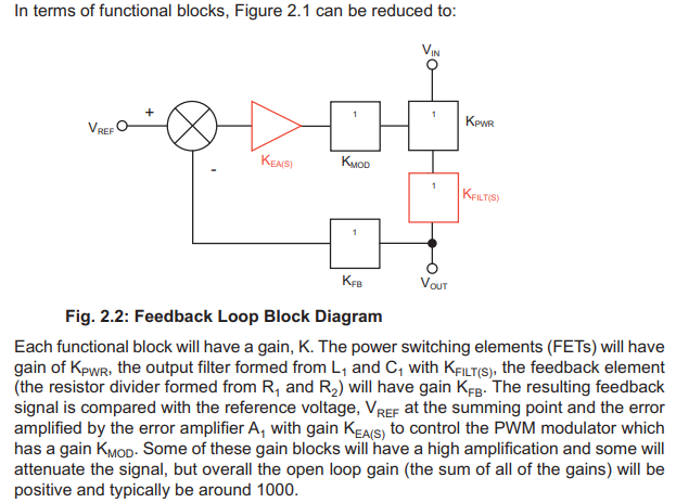
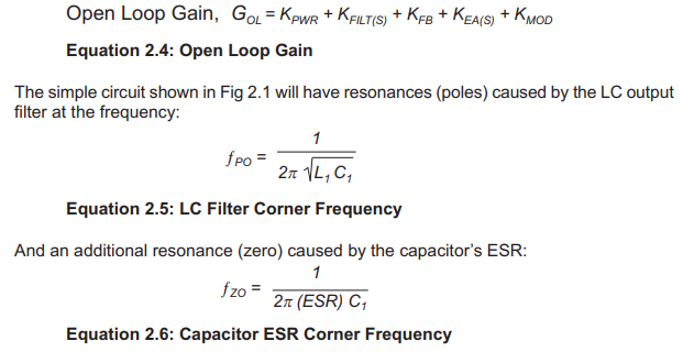
DC/DC Book of Knowledge Practical tips for the User
Book of Knowledge by Steve Roberts.pdf (dialogue.sk)
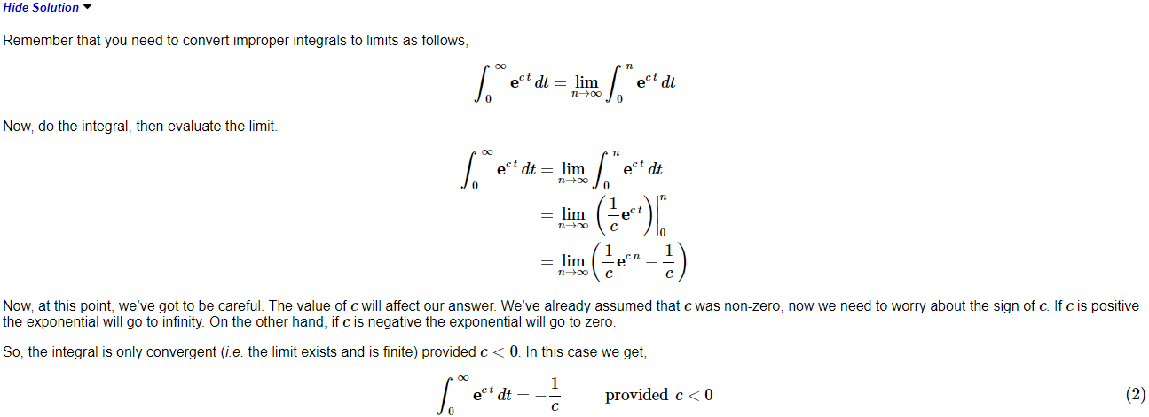
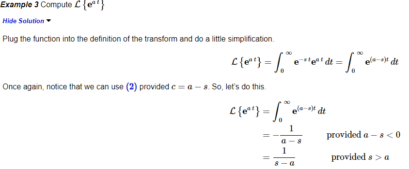
Laplace transform
Differential Equations - The Definition (lamar.edu)
Definition
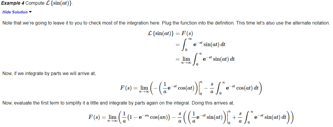
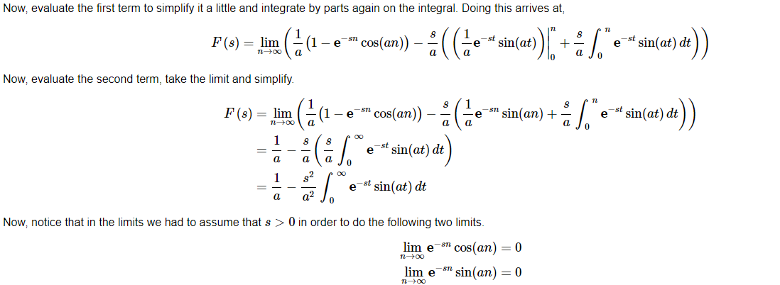
Suppose that f(t)f(t) is a piecewise continuous function. The Laplace transform of f(t)f(t) is denoted L{f(t)}L{f(t)} and defined as

There is an alternate notation for Laplace transforms. For the sake of convenience we will often denote Laplace transforms as,
![]()


Closed-loop transfer function
https://en.wikipedia.org/wiki/Closed-loop_transfer_function
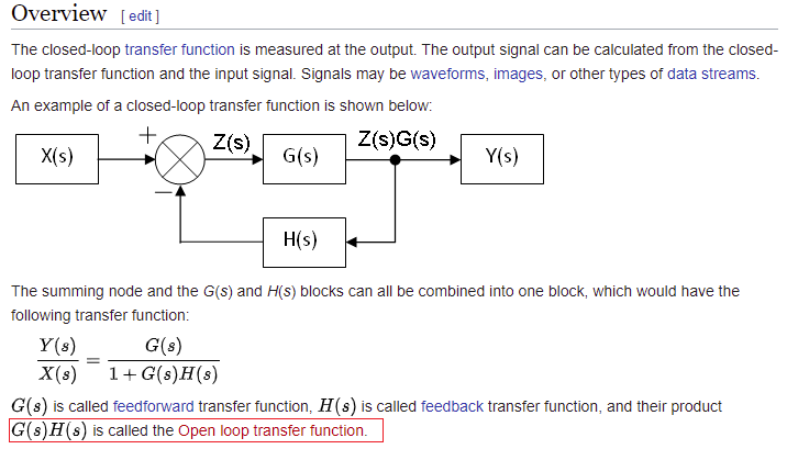
A closed-loop transfer function in control theory is a mathematical expression (algorithm) describing the net result of the effects of a closed (feedback) loop on the input signal to the plant under control.
Derivation
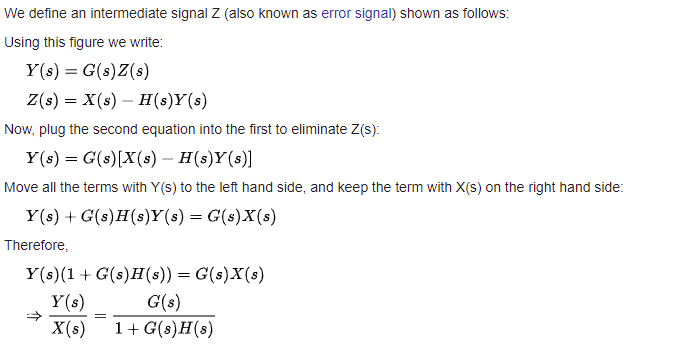
https://en.wikipedia.org/wiki/Control_theory#Closed-loop_transfer_function
Closed-loop transfer function
https://en.wikipedia.org/wiki/Control_theory#Closed-loop_transfer_function

If we assume the controller C, the plant P, and the sensor F are linear and time-invariant (i.e., elements of their transfer function C(s), P(s), and F(s) do not depend on time), the systems above can be analysed using the Laplace transform on the variables. This gives the following relations:

The numerator is the forward (open-loop) gain from r to y, and the denominator is one plus the gain in going around the feedback loop, the so-called loop gain. If ![]() , i.e., it has a large norm with each value of s, and if
, i.e., it has a large norm with each value of s, and if ![]() , then Y(s) is approximately equal to R(s) and the output closely tracks the reference input.
, then Y(s) is approximately equal to R(s) and the output closely tracks the reference input.
The open-loop continuous-time system transfer function
chapter4_BD.pdf (rutgers.edu)
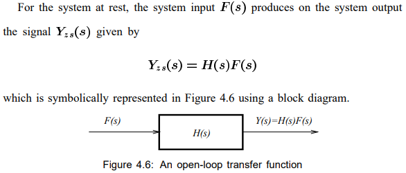
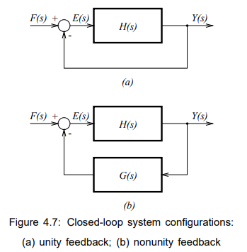
Unity feedback
Following signals in the block diagram in the direction of the arrows,we can find the closed-loop system transfer function from ![]() to
to ![]() , assuming zero initial conditions
, assuming zero initial conditions
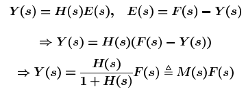

Nonnity feedback
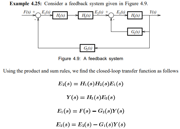
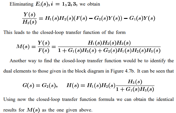
The defined closed-loop transfer function is called the closed-loop transfer function with unity feedback. In many applications, in the feedback loop another transfer function is present, see Figure 4.7b. The closed-loop transfer function with non unity feedback is obtained similarly as follows

Definition 4.1: The closed-loop system transfer function for non unity feedback is defined by

The cascade connection of open-loop transfer functions is shown in Figure 4.8a.
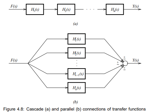
It is easy to conclude that the equivalent open-loop transfer function is given by the product of elementary open-loop transfer functions
![]()
This formula is called the product rule for elementary open-loop transfer functions.
The parallel connection of the open-loop transfer functions is represented in Figure 4.8b. Its equivalent open-loop transfer function is equal to the sum of elementary open-loop transfer functions, that is
![]()
The last formula is called the sum rule for elementary open-loop transfer functions.
Understanding Poles and Zeros
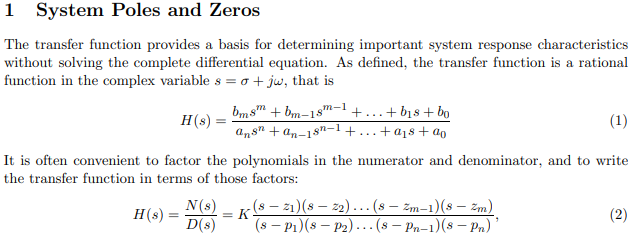
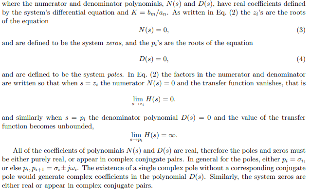
PoleZero.dvi (mit.edu)
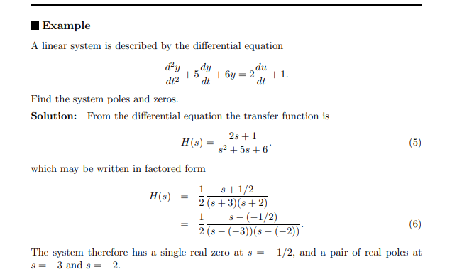
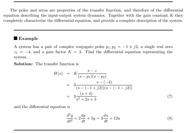
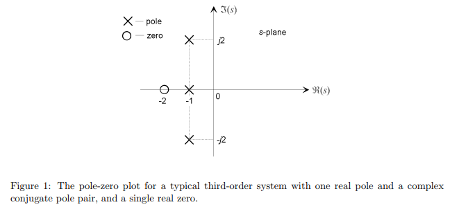
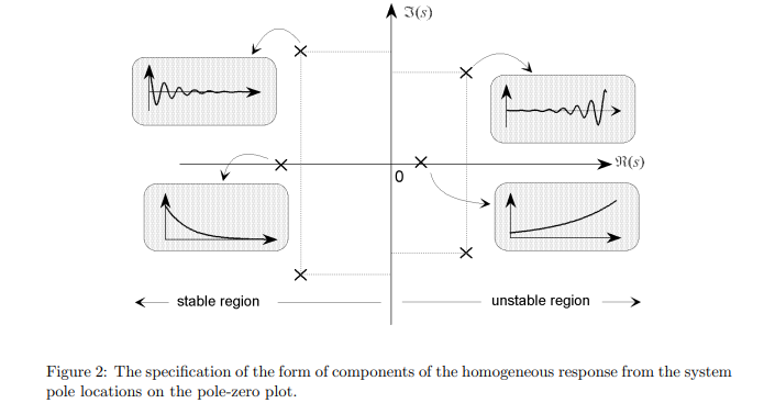
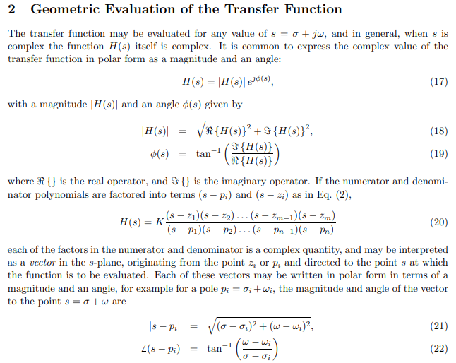
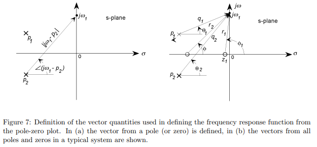
2 Geometric Evaluation of the Transfer Function

11.5: Poles and Zeros in the S-Plane
11.5: Poles and Zeros in the S-Plane - Engineering LibreTexts
Once the Laplace-transform of a system has been determined, one can use the information contained in function's polynomials to graphically represent the function and easily observe many defining characteristics. The Laplace-transform will have the below structure, based on Rational Functions (Section 12.7):

The two polynomials, P(s)P(s) and Q(s)Q(s), allow us to find the poles and zeros of the Laplace-Transform.
Definition: zeros
- The value(s) for ss where P(s)=0.
- The complex frequencies that make the overall gain of the filter transfer function zero.
Definition: poles
- The value(s) for ss where Q(s)=0.
- The complex frequencies that make the overall gain of the filter transfer function infinite.

The S-Plane
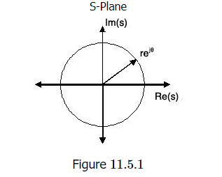
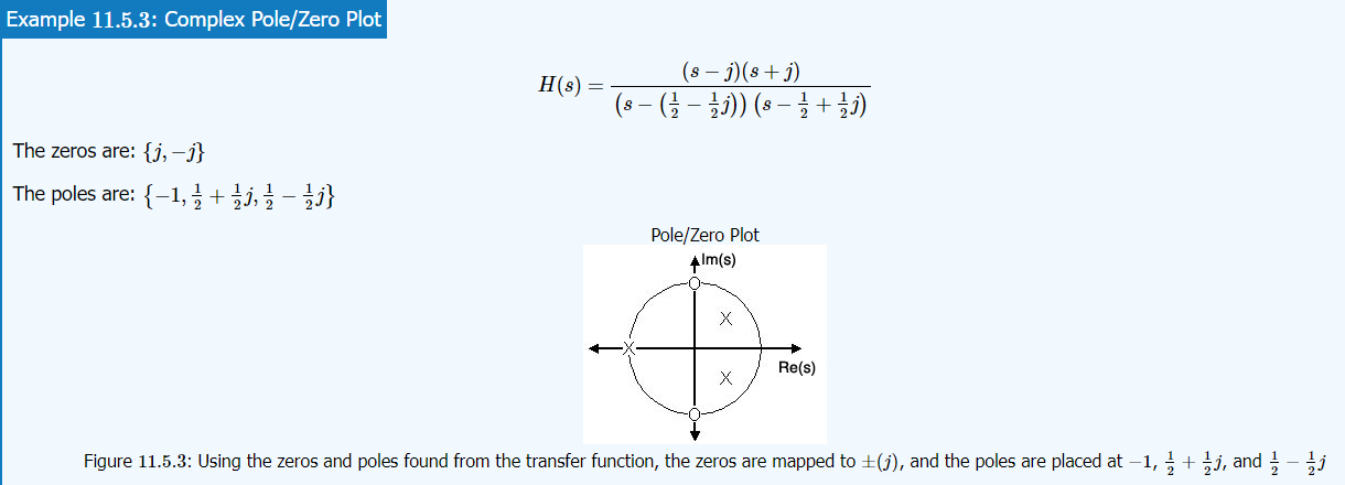
Once the poles and zeros have been found for a given Laplace Transform, they can be plotted onto the S-Plane. The S-plane is a complex plane with an imaginary and real axis referring to the complex-valued variable zz. The position on the complex plane is given by rejθrejθ and the angle from the positive, real axis around the plane is denoted by θθ. When mapping poles and zeros onto the plane, poles are denoted by an "x" and zeros by an "o". The below figure shows the S-Plane, and examples of plotting zeros and poles onto the plane can be found in the following section.

最后
以上就是甜美草丛最近收集整理的关于Loop Response Considerations in Peak Current Mode Buck Converter Design1 Introduction2 Peak Current Mode Loop ModelingLaplace transformDifferential Equations - The Definition (lamar.edu)Closed-loop transfer functionThe open-loop continuous-time syste的全部内容,更多相关Loop内容请搜索靠谱客的其他文章。


发表评论 取消回复