https://www.ti.com.cn/cn/lit/an/sloa020a/sloa020a.pdf?ts=1640863691642&ref_url=https%253A%252F%252Fwww.google.com%252F https://www.ti.com.cn/cn/lit/an/sloa020a/sloa020a.pdf?ts=1640863691642&ref_url=https%253A%252F%252Fwww.google.com%252F
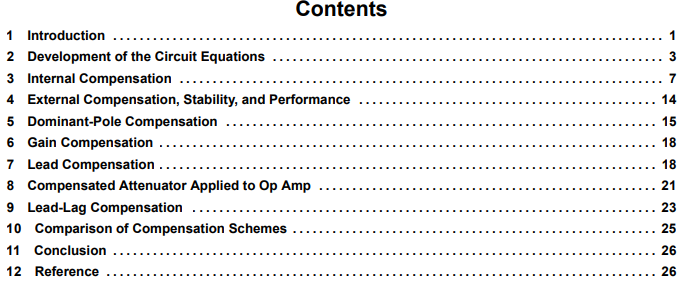
2 Development of the Circuit Equations

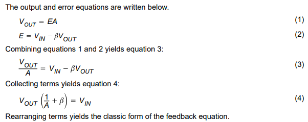
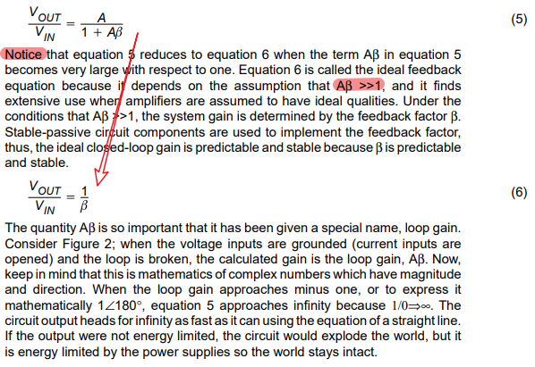
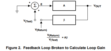

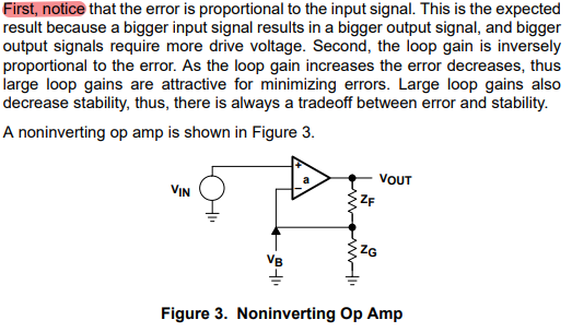
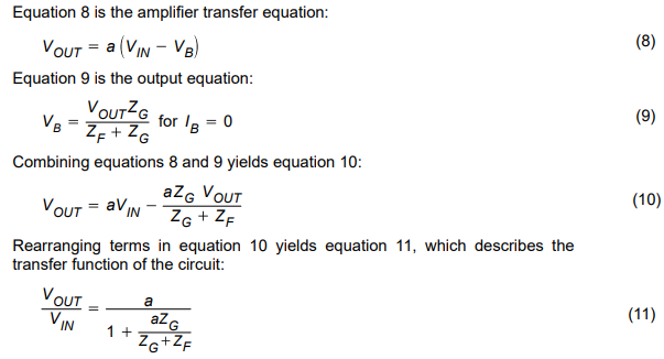
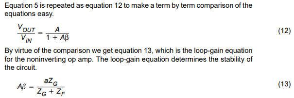
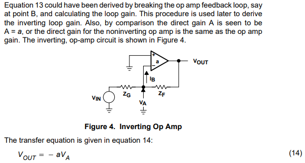
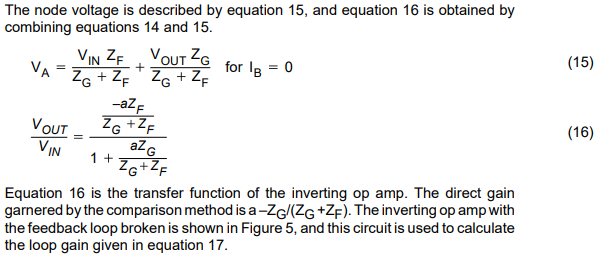
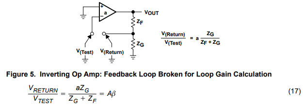
A Several things must be mentioned at this point in the analysis. First, the transfer functions for the noninverting and inverting equations, 11 and 16, are different. For a common set of ZG and ZF values, the magnitude and polarity of the gains are different. Second, the loop gain of both circuits, as given by equations 13 and 17, is identical. Thus, the stability performance of both circuits is identical although their transfer equations are different. This makes the important point that stability is not dependent on the circuit inputs. Third, the A gain block shown in Figure 1 is different for each op-amp circuit. By comparison of equations 5, 11, and 16 we see that ANON–INV = a and AINV = aZF ÷ (ZG + ZF). Equation 7 shows that the error is inversely proportional to the loop gain; thus, the accuracy of identical closed-loop gain inverting and noninverting op-amp circuits is different. Equation 17 is used to compensate all op amp circuits. First, we determine what compensation method to use. Second, we derive the compensation equations. Third, we analyze the closed-loop transfer function to determine how it is modified by the compensation. The effect of the compensation on the closed-loop transfer function often determines which compensation technique will be used.
3 Internal Compensation
Op amps are internally compensated to save external components and to enable their use by less knowledgeable people. It takes some measure of analog knowledge to compensate an analog circuit. Internally compensated op amps normally are stable when they are used in accordance with the applications instructions. Internally compensated op amps are not unconditionally stable. They are multiple pole systems, but they are internally compensated such that they appear as a single pole system over much of the frequency range. The cost of internal compensation is that it severely decreases the closed-loop bandwidth of the op amp.
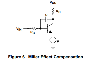
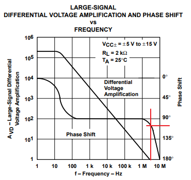
Internal compensation is accomplished in several ways, but the most common method is to connect a capacitor across the collector-base junction of a voltage gain transistor (see Figure 6). The Miller effect multiplies the capacitor value by an amount approximately equal to the stage gain, thus, the Miller effect uses small value capacitors for compensation. Figure 7 shows the gain/phase diagram for an older op amp (TL03X). When the gain crosses the 0-dB axis (gain equal to one) the phase shift is about 100°, thus, the op amp must be modeled as a second order system because the phase shift is more than 90°.
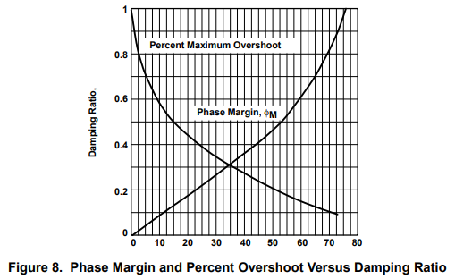
This yields a phase margin of φ = 180° – 100° = 80°, thus the circuit should be very stable (Reference 1 explains feedback analysis tools). Referring to Figure 8, the damping ratio is one and the expected overshoot is zero. Figure 7 shows approximately 10% overshoot which is unexpected, but inspecting Figure 7 further reveals that the loading capacitance for the two plots is different. The pulse response is loaded with 100 pF rather than 25 pF shown for the gain/phase plot, and this extra loading capacitance accounts for the loss of phase margin.
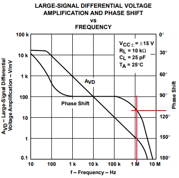
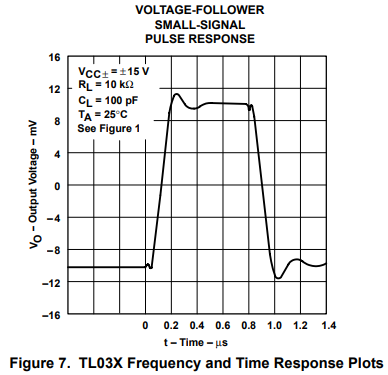
Why does the loading capacitance make the op amp unstable? Look closely at the gain/phase response between 1 MHz and 9 MHz, and observe that the gain curve changes slope drastically while the rate of phase change approaches 120°/decade. The radical gain/phase slope change proves that several poles are located in this area. The loading capacitance works with the op-amp output impedance to form another pole, and the new pole reacts with the internal op-amp poles. As the loading capacitor value is increased, its pole migrates down in frequency, causing more phase shift at the 0-dB crossover frequency. The proof of this is given in the TL03X data sheet where plots of ringing and oscillation versus loading capacitance are shown.
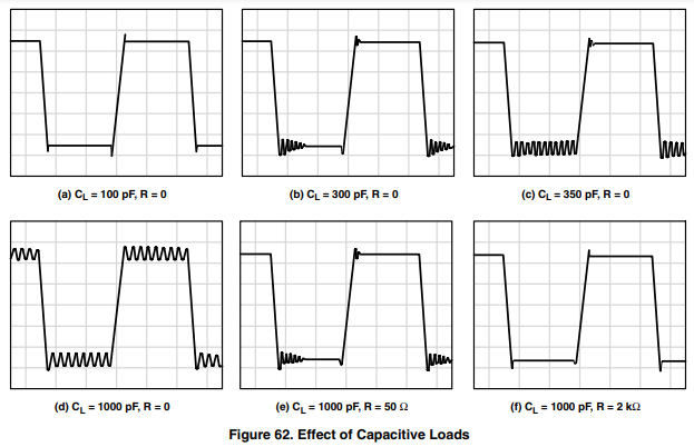
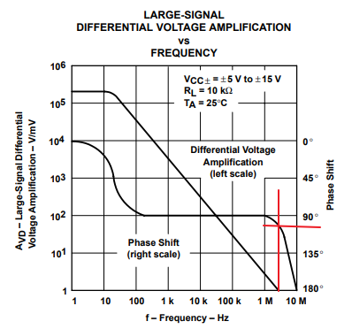
Figure 9 shows similar plots for the TL07X which is the newer family of op amps. Notice that the phase shift is 100 when the gain crosses the 0-dB axis. This yields a phase margin of 80, which is close to being unconditionally stable. The slope of the phase curve changes to 180/decade about one decade from the 0-dB crossover point. The radical slope change causes suspicion about the 90° phase margin. Furthermore, the gain curve must be changing radically when the phase is changing radically. The gain/phase plot may not be totally false, but it sure is overly optimist
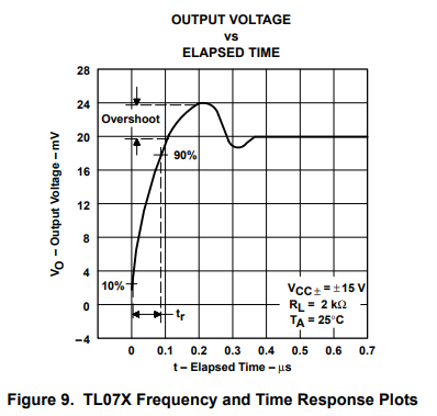
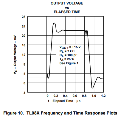
The TL07X pulse response plot shows approximately 20% overshoot. There is no loading capacitance indicated on the plot to account for a seemingly unconditionally stable op amp exhibiting this large an overshoot. Something is wrong here: the analysis is wrong, the plots are wrong, or the parameters are wrong. Figure 10 shows the plots for the TL08X family of op amps which are sisters to the TL07X family. The gain/phase curve and pulse response is virtually identical, but the pulse response lists a 100-pF loading capacitor. This little exercise illustrates three valuable points: first, if the data seems wrong it probably is wrong, second, even the factory people make mistakes, and third, the loading capacitor makes op amps ring, overshoot, or oscillate.
The frequency and time-response plots for the TLV277X family of op amps is shown in Figures 11 and 12. First, notice that the information is more sophisticated because the phase response is given in degrees of phase margin; second, both gain/phase plots are done with substantial loading capacitors (600 pF), so they have some practical value; and third, the phase margin is a function of power supply voltage.
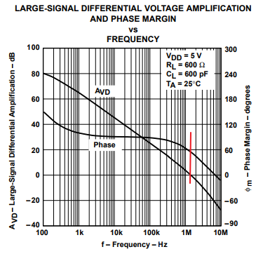
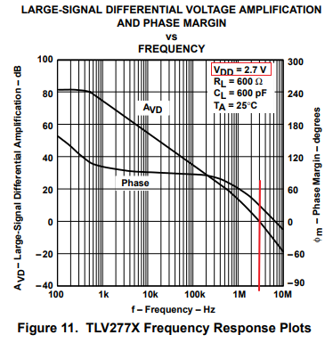
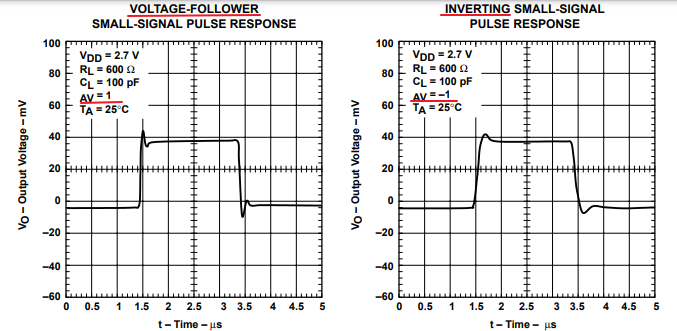
At VCC = 5 V, the phase margin at the 0-dB crossover point is 60°, while it is 30° at VCC = 2.7 V. This translates into an expected overshoot of 18% at VCC = 5 V, and 28% at VCC = 2.7 V. Unfortunately, the time response plots are done with 100-pF loading capacitance, hence we can not check our figures very well. The VCC = 2.7-V overshoot is approximately 2%, and it is almost impossible to figure out what the overshoot would have been with a 600-pF loading capacitor. The small-signal pulse response is done with mV-signals, and that is a more realistic measurement than using the full-signal swing.
Internally compensated op amps are very desirable because they are easy to use, and they do not require external compensation components. Their drawback is that the bandwidth is limited by the internal compensation scheme. The op-amp open-loop gain eventually (when it shows up in the loop gain) determines the error in an op-amp circuit. In a noninverting buffer configuration, the TL277X is limited to 1% error at 50 kHz (VCC = 2.7 V) because the op amp gain is 40 dB at that point. Circuit designers can play tricks such as bypassing the op amp with a capacitor to emphasize the high-frequency gain, but the error is still 1%. Keep equation 7 in mind because it defines the error. If the TLV277X were not internally compensated, it could be externally compensated for a lower error at 50 kHz because the gain would be much higher.
4 External Compensation, Stability, and Performance
This section is approached on a compensation type basis. Nobody compensates an op amp because it is there; they have a reason to compensate the op amp, and that reason is usually stability. They want the op amp to perform a function in a circuit where it is potentially unstable. Internally and noninternally compensated op amps are compensated externally because certain circuit configurations do cause oscillations. Several potentially unstable circuit configurations are analyzed in this section, and the reader can extend the external compensation techniques as required.
Other reasons for externally compensating op amps are noise reduction, flat amplitude response, and obtaining the highest bandwidth possible from an op amp. An op amp generates noise, and noise is generated by the system. The noise contains many frequency components, and when a high-pass filter is incorporated in the signal path, it reduces high-frequency noise. Compensation can be employed to roll off the op amp’s high-frequency, closed-loop response, thus, causing the op amp to act as a noise filter. Internally compensated op amps are modeled with a second order equation, and this means that the output voltage can overshoot in response to a step input. When this overshoot (or peaking) is undesirable, external compensation can increase the phase margin to 90° where there is no peaking. An uncompensated op amp has the highest bandwidth possible. External compensation is required to stabilize uncompensated op amps, but the compensation can be tailored to the specific circuit, thus yielding the highest possible bandwidth consistent with the pulse response requirements.
5 Dominant-Pole Compensation
We saw that capacitive loading caused potential instabilities, thus, an op amp loaded with an output capacitor is a circuit configuration that must be analyzed. This circuit is called dominant pole compensation because if the pole formed by the op amp output impedance and the loading capacitor is located close to the zero frequency axis, it becomes dominant. The op-amp circuit is shown in Figure 13, and the open-loop circuit used to calculate the loop gain (Aβ) is shown in Figure 14.
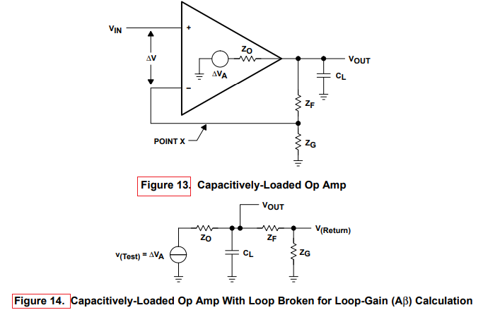
Thevenin equivalent circuit
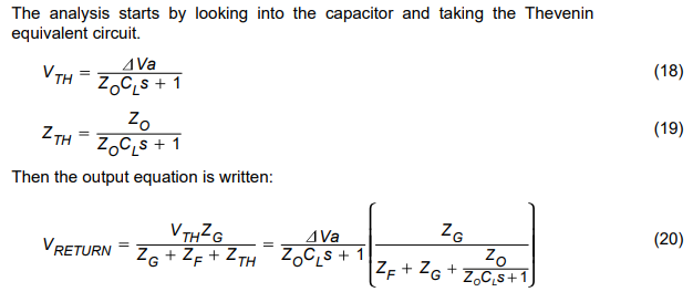
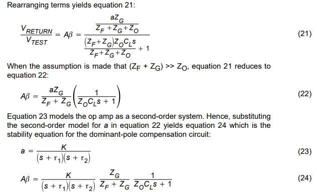
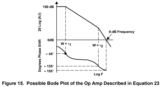
Several conclusions can be drawn from equation 24 depending on the location of the poles. If the Bode plot of equation 23, the op amp transfer function, looks like that shown in Figure 15, it only has 25° phase margin, and there is approximately 48% overshoot. When the pole introduced by ZO and CL moves towards the zero frequency axis it comes close to the τ2 pole, and it adds phase shift to the system. Increased phase shift increases peaking and decreases stability. In the real world, many loads, especially cables, are capacitive, and an op amp like the one pictured in Figure 15 would ring while driving a capacitive load. The load capacitance causes peaking and instability in internally compensated op amps when the op amps do not have enough phase margin to allow for the phase shift introd
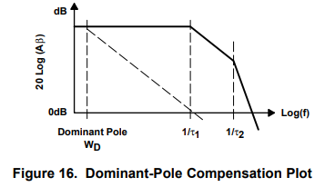
Prior to compensation, the Bode plot of an uncompensated op amp looks like that shown in Figure 16. Notice that the break points are located close together thus accumulating about 180° of phase shift before the 0 dB crossover point; the op amp is not usable and probably unstable. Dominant pole compensation is often used to stabilize these op amps. If a dominant pole, in this case ωD, is properly placed it rolls off the gain so that τ1 introduces 45 phase at the 0 dB crossover point. After the dominant pole is introduced the op amp is stable with 45° phase margin, but the op-amp gain is drastically reduced for frequencies higher than ωD. This procedure works well for internally compensated op amps, but is seldom used for externally compensated op amps because inexpensive discrete capacitors are readily available
6 Gain Compensation
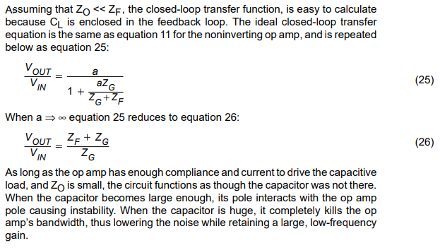
When the closed-loop gain of an op-amp circuit is related to the loop gain, as it is in voltage feedback op amps, the gain can be used to stabilize the circuit. This type of compensation can not be used in current feedback op amps because the mathematical relationship between the loop gain and ideal closed-loop gain does not exist. The loop gain equation is repeated as equation 27. Notice that the closed-loop gain parameters ZG and ZF are contained in equation 27, hence the stability can be controlled by manipulating the closed-loop gain parameters.

The original loop-gain curve for a closed-loop gain of one is shown in Figure 17, and it is or comes very close to being unstable. If the closed-loop noninverting gain is changed to 9, then K changes from K/2 to K/10. The loop-gain intercept on the Bode plot (see Figure 17) moves down 14 dB, and the circuit is stabilized.
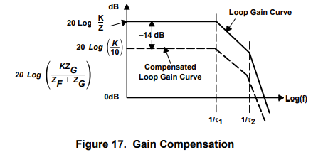
Gain compensation works for inverting or noninverting op-amp circuits because the loop gain equation contains the closed-loop gain parameters in both cases. When the closed-loop gain is increased, the accuracy and the bandwidth decrease. As long as the application can stand the higher gain, gain compensation is the best type of compensation to use. Uncompensated versions of normally internally compensated op amps are offered for sale as stable op amps with minimum gain restrictions. As long as the gain in the circuit you design exceeds the gain specified, this is economical and a safe mode of operatio
7 Lead Compensati
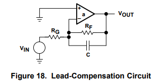

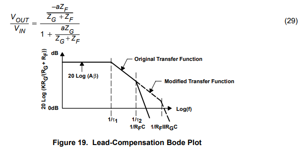
The compensation capacitor introduces a pole and zero into the loop equation. The zero always occurs before the pole because RF >RF||RG. When the zero is properly placed it cancels out the τ2 pole along with its associated phase shift. The original transfer function is shown in Figure 19, drawn as solid lines. When the RFC zero is placed at ω = 1/τ2, it cancels out the τ2 pole causing the Bode plot to continue on a slope of –20 dB/decade. When the frequency gets to ω = 1/(RF||RG)C, this pole changes the slope to –40 dB/decade. Properly placed, the capacitor aids stability, but what does it do to the closed-loop transfer function? The equation for the inverting op amp closed-loop gain is repeated below.

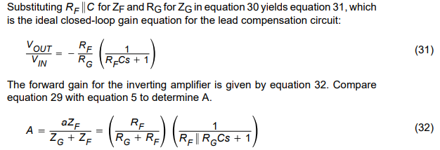
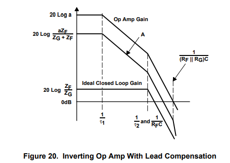
The op-amp gain (a) the forward gain (A) and the ideal closed-loop gain are plotted in Figure 20. The op-amp gain is plotted for reference only. The forward gain for the inverting op amp is not the op-amp gain. Notice that the forward gain is reduced by the factor RF/(RG +RF), and it contains a high-frequency pole. The ideal closed-loop gain follows the ideal curve until the 1/RFC breakpoint (same location as 1/τ2 breakpoint), and then it slopes down at –20 dB/decade. Lead compensation sacrifices the bandwidth between the 1/RFC breakpoint and the forward gain curve. The location of the 1/RFC pole determines the bandwidth sacrifice, and it can be much greater than shown here. The pole caused by RF, RG, and C does not appear until the op amp’s gain has crossed the 0 dB axis, thus, it does not effect the ideal closed-loop transfer function.

The plot of the noninverting op amp with lead compensation is shown in Figure 21. There is only one plot for both the op-amp gain (a) and the forward gain (A), because they are identical in the noninverting circuit configuration. The ideal starts out as a flat line, but it slopes down because its closed-loop gain contains a pole and a zero. The pole always occurs closer to the low-frequency axis because RF > RF||RG. The zero flattens the ideal closed-loop gain curve, but it never does any good because it can not fall on the pole. The pole causes a loss in the closed-loop bandwidth by the amount separating the closed-loop and forward-gain curves.
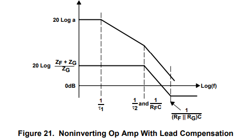
Although the forward gain is different in the inverting and noninverting circuits, the closed-loop transfer functions take very similar shapes. This becomes truer as the closed-loop gain increases because the noninverting forward gain approaches the op-amp gain. This relationship can not be relied on in every situation, and each circuit must be checked to determine the closed-loop effects of the compensation scheme.
8 Compensated Attenuator Applied to Op Amp
Stray capacitance on op-amp inputs is a problem that circuit designers are always trying to get away from because it decreases closed-loop frequency response or causes peaking. The circuit shown in Figure 22 has some stray capacitance (CG) connected from the inverting input to ground. Equation 34 is the loop-gain equation for the circuit with input capacitance.
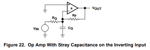

Op amps having high input and feedback resistors are subject to instability caused by stray capacitance on the inverting input. Referring to equation 34, when the 1/(RF||RGCG) pole moves close to τ2 the stage is set for instability. Reasonable component values for a CMOS op amp are RF = 1 MΩ, RG = 1 MΩ, and CG = 10 pF. The resulting pole occurs at 318 kHz, and this frequency is lower than the breakpoint of τ2 for many op amps. There is 90 phase shift resulting from τ1, the 1/(RF||RGC) pole adds 45° phase shift at 318 kHz, and τ2 adds another 45° phase shift at about 600 kHz. This circuit is unstable because of the stray input capacitance. The circuit is compensated by adding a feedback capacitor as shown in Figure 23.
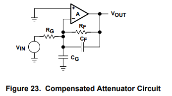
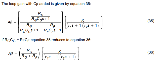
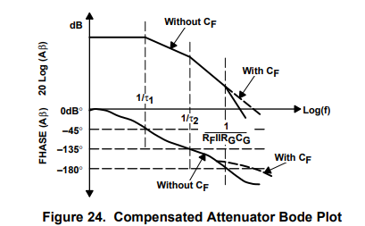
The compensated attenuator Bode plot is shown in Figure 24. Adding the correct 1/RFCF breakpoint cancels out the 1/RGCG breakpoint, the loop gain is independent of the capacitors. Now is the time to take advantage of the stray capacitance. CF can be formed by running a wide copper strip from the output of the op amp over the ground plane under RF; do not connect the other end of this copper strip. The circuit is tuned by removing some copper (a razor works well) until all peaking is eliminated. Then measure the copper, and have an identical trace put on the print-circuit board.
The inverting and noninverting closed-loop gain equations are a function of frequency. Equation 37 is the closed-loop gain equation for the inverting op amp. When RFCF = RGCG equation 37 reduces to equation 38 which is independent of the breakpoint. This also happens to the noninverting op-amp circuit. This is one of the few occasions when the compensation does not affect the closed-loop gain frequency response.

9 Lead-Lag Compensation
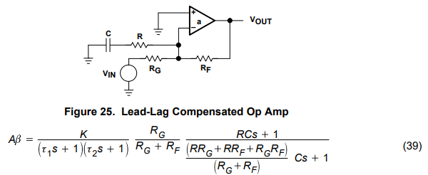
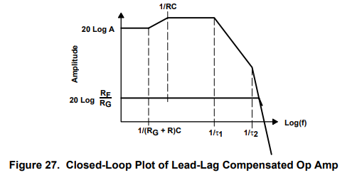
Referring to Figure 26, a pole is introduced at ω = 1/RC, and this pole reduces the gain 3 dB at the breakpoint. When the zero occurs prior to the first op-amp pole it cancels out the phase shift caused by the ω = 1/RC pole. The phase shift is completely canceled before the second op-amp pole occurs, and the circuit reacts as if the pole was never introduced. Nevertheless, Aβ is reduced by 3 dB or more, so the loop gain crosses the 0-dB axis at a lower frequency. The beauty of lead-lag compensation is that the closed-loop ideal gain is not affected as is shown below. The Thevenin equivalent of the input circuit is calculated in equation 40, the circuit gain in terms of Thevenin equivalents is calculated in equation 41, and the ideal closed-loop gain is calculated in equation 42.
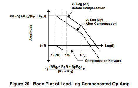
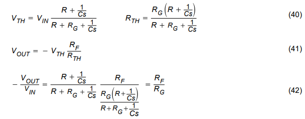
RG Equation 42 is intuitively obvious because the RC network is placed across a virtual ground. As long as the loop gain (Aβ) is large, the feedback will null out the closed-loop effect of RC, and the circuit will function as if it weren’t there. The closed-loop log plot of the lead-lag compensated op amp is given in Figure 27. Notice that the pole and zero resulting from the compensation occur and are gone before the first amplifier poles come on the scene. This prevents interaction, but it is not required for stability.
10 Comparison of Compensation Schemes
Internally compensated op amps can, and often do, oscillate under some circuit conditions. Internally compensated op amps need an external pole to get the oscillation or ringing started, and circuit stray capacitances often supply the phase shift required for instability. Loads, such as cables, often cause internally compensated op amps to ring severely.
Dominant pole compensation is often used in IC design because it is easy to implement. It rolls off the closed-loop gain early; thus, it is seldom used as an external form of compensation unless filtering is required. Load capacitance, depending on its pole location, usually causes the op amp to ring. Large load capacitance can stabilize the op amp because it acts as dominant pole compensation.
The simplest form of compensation is gain compensation. High, closed-loop gains are reflected in lower-loop gains, and in turn, lower-loop gains increase stability. If an op-amp circuit can be stabilized by increasing the closed-loop gain, do it.
Stray capacitance across the feedback resistor tends to stabilize the op amp because it is a form of lead compensation. This compensation scheme is useful for limiting the circuit bandwidth, but it decreases the closed-loop gain.
Stray capacitance on the inverting input works with the parallel combination of the feedback and gain setting resistors to form a pole in the Bode plot, and this pole decreases the circuit’s stability. This effect is normally observed in highimpedance circuits built with CMOS op amps. Adding a feedback capacitor forms a compensated attenuator scheme which cancels out the input pole. The cancellation occurs when the input and feedback RC time constants are equal. Under the conditions of equal time constants, the op amp functions as though the stray input capacitance was not there. An excellent method of implementing a compensated attenuator is to build a stray feedback capacitor using the ground plane and a trace off the output node.
Lead-lag compensation stabilizes the op amp, and it yields the best closed-loop frequency performance. Contrary to some published opinions, no compensation scheme will increase the bandwidth beyond that of the op amp. Lead-lag compensation just gives the best bandwidth for the compensation.
11 Conclusion
The stability criteria often is not oscillation, rather, it is circuit performance as exhibited by peaking and ringing.
The circuit bandwidth can often be increased by connecting an external capacitor in parallel with the op amp. Some op amps have hooks which enable a parallel capacitor to be connected in parallel with a portion of the input stages. This increases bandwidth because it shunts high frequencies past the low bandwidth gm stages, but this method of compensation depends on the op amp type and manufacturer.
The compensation techniques given here are adequate for the majority of applications. When the new and challenging application presents itself, use the procedure outline here to invent your own compensation technique.
Other reference
TL03x, TL03xA ENHANCED-JFET LOW-POWER LOW-OFFSET OPERATIONAL AMPLIFIERS
https://www.ti.com/lit/ds/symlink/tl032a.pdf?ts=1640900989080&ref_url=https%253A%252F%252Fwww.google.com%252F
control systems engineering - Books
http://freedownloads88.weebly.com/uploads/1/3/6/2/13624622/control_systems.pdf
CONTROL SYSTEM ENGINEERING-I
https://www.vssut.ac.in/lecture_notes/lecture1423904331.pdf
1.0 Introduction to Control system 1.1 Scope of Control System Engineer 1.2 Classification of Control System 1.3 Historical development of Control system 1.4 Analogues systems 1.5 Transfer function of Systems 1.6 Block diagram representation 1.7 Signal Flow Graph(SFG)
2.0 Feedback Characteristics of Control systems and sensitivity measures 2.1 The Concept of Feedback and Closed loop control 2.2 Merits of using Feedback control system 2.3 Regenerative Feedback
3.0Control System Components 3.1 Potentiometers 3.2 DC and AC Servomotors 3.3 Tachometers 3.4 Amplidyne 3.5 Hydralulic systems 3.6 Pneumatic systems 3.7 Stepper Motors
4.0 Time Domain Performance Analysis of Linear Control Systems 4.1 Standard Test Signals 4.2 Time response of 1st order Systems 4.3 Unit step response of a prototype 2nd order system 4.4 Unit Ramp response of a second order system 4.4 Performance Specification of Linear System in Time domain 4.5 The Steady State Errors and Error Constants 4.6 Effect of P, PI, PD and PID Controller 4.7 Effect of Adding a zero to a system 4.8 Performance Indices(ISE,ITSE,IAE, ITAE) 4.9 Approximations of Higher order Systems by Lower order Problems
5.0 The Stability of Linear Control Systems 5.1 The Concept of Stability 5.2 The Routh Hurwitz Stability Criterion 5.3 Relative stability analysis
6.0 Root Locus Technique 6.1 Angle and Magnitude Criterion 6.2 Properties of Root Loci 6.3 Step by Step Procedure to Draw Root Locus Diagram 6.4 Closed Loop Transfer Function and Time Domain response 6.5 Determination of Damping ratio, Gain Margin and Phase Margin from Root Locus 6.6 Root Locus for System with transportation Lag. 6.7 Sensitivity of Roots of the Characteristic Equation.
7.0 Frequency Domain Analysis. 7.1 Correlation between Time and frequency response 7.2 Frequency Domain Specifications 7.3 Polar Plots and inverse Polar plots 7.4 Bode Diagrams 7.4.1 Principal factors of Transfer function 7.4.2 Procedure for manual plotting of Bode Diagram 7.4.3 Relative stability Analysis 7.4.4 Minimum Phase, Non-minimum phase and All pass systems 7.5 Log Magnitude vs Phase plots. 7.6 Nyquist Criterion 7.6.1 Mapping Contour and Principle of Argument 7.6.2 Nyquist path and Nyquist Plot 7.6.3 Nyquist stability criterion 7.6.4 Relative Stability: Gain Margin, and Phase Margin 7.7 Closed Loop Frequency Response 7.7.1 Gain Phase Plot 7.7.1.1 Constant Gain(M)-circles 7.7.1.2 Constant Phase (N) Circles 7.7.1.3 Nichols Chart 7.8 Sensitivity Analysis in Frequency Domain
Application Note AN-1162 Compensator Design Procedure for Buck Converter with Voltage-Mode Error-Amplifier
https://www.infineon.com/dgdl/an-1162.pdf?fileId=5546d462533600a40153559a8e17111a
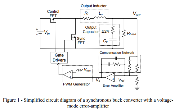
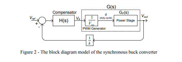
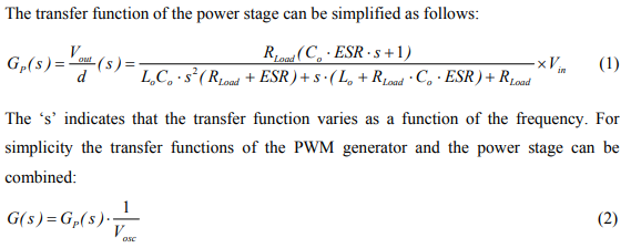
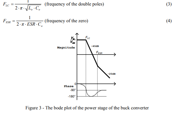
Therefore, G(s) is usually referred to as the transfer function of the power stage. The roots of the polynomial in the denominator of (1) are called the poles of the transfer function of the power stage. Similarly the roots of the numerator of (1) are the zeros of the transfer function of the power stage. The transfer function of the power stage is a second order system with a double pole at the resonance frequency (of the LC filter) and a zero produced by the ESR of the output capacitor. The resonance frequency and the zero frequency associated with the ESR are given by (3) and (4). The approximate Bode plot of the power stage is sketched in Figure 3. The double pole causes the gain to fall with a slope of -40dB/dec up to the zero frequency ( FESR ) which compensates one of the poles. The zero frequency is a characteristic parameter of the output capacitor and is dependant on the type of the capacitor used. This frequency can be as low as a few kHz for an electrolytic capacitor to as high as a few MHz for a ceramic capacitor. More information about designing the power stage is provided in Appendix A.
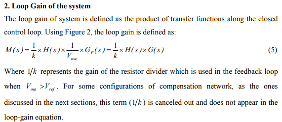
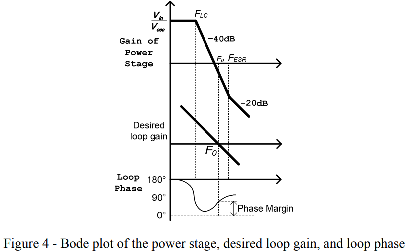
The bode plots of power stage and desired loop gain is shown in Figure 4, where F0 is the zero crossover frequency defined as the frequency when loop gain equals unity. F0 is also called “the bandwidth of the loop” or “the bandwidth of the system”.
Typically, F0 can be set to 1/10~1/5 of the switching frequency. The speed of the system response to load transients is determined by F0 . In other words, the higher the crossover frequency, the faster the load transient response would be. However, the crossover frequency should be low enough to allow attenuation of switching noise. The slope of the loop gain at F0 should be about –20dB in order to ensure a stable system. The phase margin should be greater than 45º for overall stability.
3. Step by step compensator design procedure
As mentioned in the Introduction, to have a stable closed loop buck converter with appropriate performance, a properly designed compensator is required. The typical procedure of compensator design is as follows:
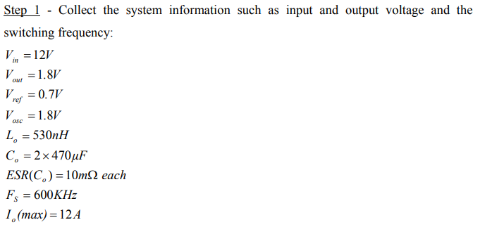
Step 1 - Collect system parameters such as input voltage, output voltage, maximum load/output current, switching frequency, input and output capacitance, and output inductance.
Step 2 - Using (3) and (4) determine the power stage poles and zero.
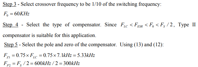
Step 3 - Determine the zero crossover frequency of the loop, F0 . Usually this frequency is chosen equal to 1/10 to 1/5 of the switching frequency.
![]()
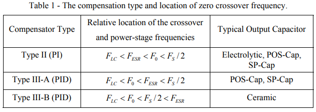
Step 4 - Determine the compensation type. The compensation type is determined by the location of zero crossover frequency and characteristics of the output capacitor as shown in Table 1.
Step 5 - Determine the desired location of the poles and zeros of the selected compensator (this will be explained for each type of compensator).
Step 6 - Calculate the real parameters (resistors and capacitors) for the selected compensator so that the desired poles/zeros are achieved. Choose the standard values for resistors and capacitors such that they are as close to the calculated values as possible.
4. Type II Compensator Design
Type II compensation is used for applications where the frequency of the zero caused by output capacitor and its ESR ( FESR ) is smaller than the closed loop bandwidth ( F0 ) as shown below:
![]()
This condition is usually met when the output capacitor is of electrolytic type. The FESR (refer to (4)) for this type of capacitor is in the range of a few kHz.
The schematic of the type II compensator is depicted in Figure 5.
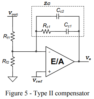
Assuming the gain/band-width of the error-amplifier (E/A) is very high, the transfer function of this compensator is given by:
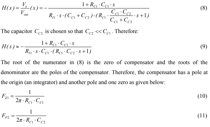
The approximate bode-plot of the power stage, the Type II compensator, and the desired loop gain has been drawn in Figure 6.
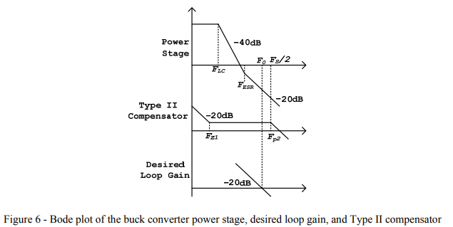
Each pole makes the phase of the loop drop by 90º and each zero makes the phase rise by 90º. The phase change of a zero/pole starts at about 1 decade below the frequency of the zero/pole and ends about 1 decade above it. It should be noted that due to negative feedback (minus sign of H(s)) initially there is 180º phase-shift in the compensator. The phase change due to poles and zeros are added to this 180º. Hence, to have a stable system, the overall phase of the loop should never become 360º/0º (or close to it) when the gain is greater than 1 (0dB). Especially, at crossover frequency ( F0 ), the phase should be at least 45º (45º phase margin).
Since the compensator has a pole at the origin, the zero of the compensator should be placed at a frequency lower than the double poles of the LC filter to make sure the phase of the loop does not drop close to 0º around FLC . Usually the following equation is used:
![]()
The second pole of the compensator should be placed higher than the cross-over frequency so that its lagging phase (phase drop) does not decrease the phase margin of the loop. On the other hand, it should be placed lower than the switching frequency, so that enough attenuation at the switching ripple is obtained. The following equation gives a reasonable compromise:
![]()
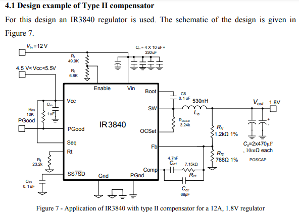
After FZ1 and Fp2 are selected the values of the components of the compensator can be calculated.
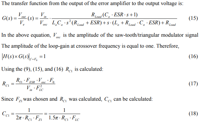
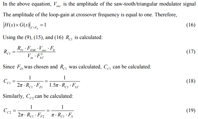
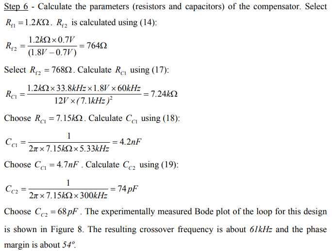
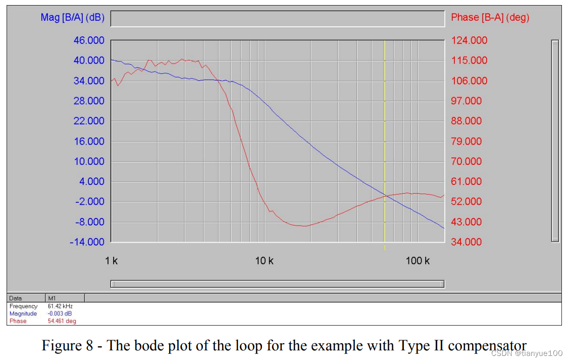
There is one degree of freedom in calculating the values of the parameters of the compensator. The procedure can be started by selecting a reasonable value for Rf1 . A value of a few kΩ should be a good starting point. Since Rf1 and Rf2 are used to set the output voltage (Figure 5), Rf2 can be calculated using the following equation:




Demystifying Type II and Type III Compensators Using OpAmp and OTA for DC/DC Converters
https://www.ti.com/lit/an/slva662/slva662.pdf
Op-Amp (Operational Transconductance Amplifier, OTA)
1 Introduction
The purpose of adding compensation to the error amplifier is to counteract some of the gains and phases contained in the control-to-output transfer function that could jeopardize the stability of the power supply. Obviously, the ultimate goal is to make the overall closed-loop-transfer function (control-to-output cascaded with the error amplifier) satisfy the stability criteria. This is to avoid having the closed-loop phase any closer to 360 degrees than the desired phase margin anywhere the gain is greater than 1 (0 dB). It is also desirable to have the slope of the gain curve at the crossover point with a value of –20 dB/decade. Phase margins of 45 degrees to 60 degrees (360 degrees minus the total closed-loop phase lag) are considered safe values that yield well-damped transient load response.
Figure 1 shows the schematic of the traditional Op-Amp with Type I configuration. The operational amplifier (the traditional Op-Amp) represents the basis of the closed-loop system. Its function, in a feedback system, is to amplify the error detected between a fixed and stable reference level and the monitored state variable
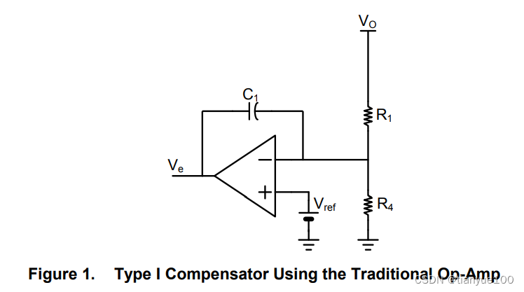
This type of Op-Amp requires local feedback (between its output and inputs) to make it stable. Under steady DC conditions, both the input terminals are virtually at the same voltage level. This determines the output voltage setting. However, though both resistors of the voltage divider affect the DC level of the converter’s output, from the AC point of view, only the upper resistor enters into the AC analysis. So the lower resistor (R4) is considered just a DC-biasing resistor, and therefore we usually ignore it in control loop (AC) analysis.
In this Type I configuration, we derive H(s) by dividing the capacitor impedance (C1) by the upper resistor (R1):

A Type I circuit built on an OTA appears in Figure 2. The voltage on the inverting pin is the converter output voltage (Vo) undergoing the voltage division brought by R1 and R4, and the amplifier output voltage (Ve) is the output current multiplied by C1 impedance.
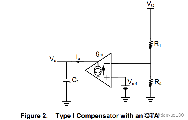
The transfer function with an OTA in this Type I configuration is given by:

The biggest change compared to the conventional Op-Amp approach is the divider network and the OTA gm parameter now enters into the equations. Regarding the divider network in the OpAmp case; thanks to the virtual ground effect, both pins were at a similar potential and the ac contribution of the lower resistor (R4) was nonexistent. In an OTA, there is no local feedback from Ve to the inverting pin, hence the absence of virtual ground. Therefore, we cannot ignore R4 any longer and the OTA gm parameter can vary depending on the care put in the integrated circuit design.
Note that the OTA model is really the simplest possible model, a voltage-controlled current source. A more complex model would feature upper and lower voltage clamp levels (given by the supply of the controller) plus a maximum output current limit. However, these extra components do not affect the AC response of the whole loop, and we can stay with the simplest representation.
If we are using an OTA, only the ratio of the feedback resistors is important. We could, for example, have a combination of 1 kΩ/5 kΩ or 10 kΩ/50 kΩ, and so on. They would all create the same gain (attenuation), and the gain-phase plot would not change. If we are using the conventional Op-Amp, the upper resistor affects the gain-phase plot. If we change that, we will get entirely different gain-phase results. Keeping the ratio unchanged does not keep the gainphase plot unchanged in this case.
In adjustable regulators with the conventional Op-Amp, if we want to change the output voltage, it is best to change the lower feedback resistor, keeping the upper resistor unchanged. That way, the DC-biasing changes, but not the gain-phase (AC) characteristics of the feedback section.
2 Type II Compensator Using Op-Amp
Offering an origin pole, one zero, and one high-frequency pole, the Type II compensator provides a phase boost up to 90 degrees. Figure 3 shows the electrical configuration, and the transfer function is obtained by calculating the impedance offered by the network placed in the Op-Amp feedback path (Zf) and dividing it by the upper resistor (R1).

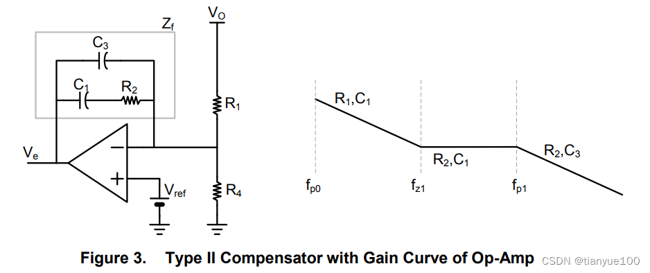
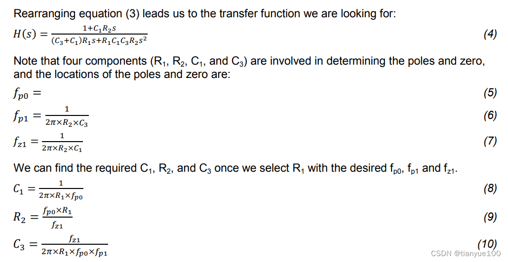
Based on the locations of the poles and zero, Figure 4 shows an example for the compensator which has an appropriate shape, and usually a good phase margin.
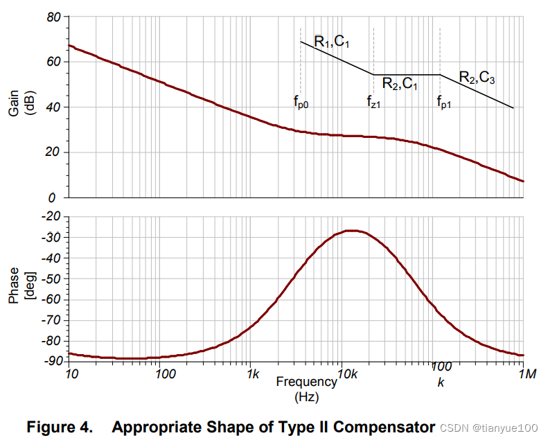
A Type II compensation amplifier adds an RC branch to flatten the gain, and improve the phase response in the mid-frequency range. The increased phase is achieved by increasing the separation of the pole and zero of the compensation.
Note that this type of compensator always has a net negative phase, and it cannot be used to improve the phase of the power stage. For this reason, Type II compensators cannot be used for voltage-mode control in CCM where there is a large phase drop just after the resonant frequency. Type II compensators are usually reserved for current-mode control compensation, or for converters that always operate in the DCM region.
3 Type II Compensator Using OTA
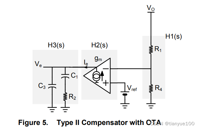
We can visualize this feedback stage as a product of three cascade transfer functions, H1(s), H2(s), and H3(s) as shown in Figure 5. It combines a pole/zero pair plus an origin pole for a high DC gain, and the transfer function is defined as:

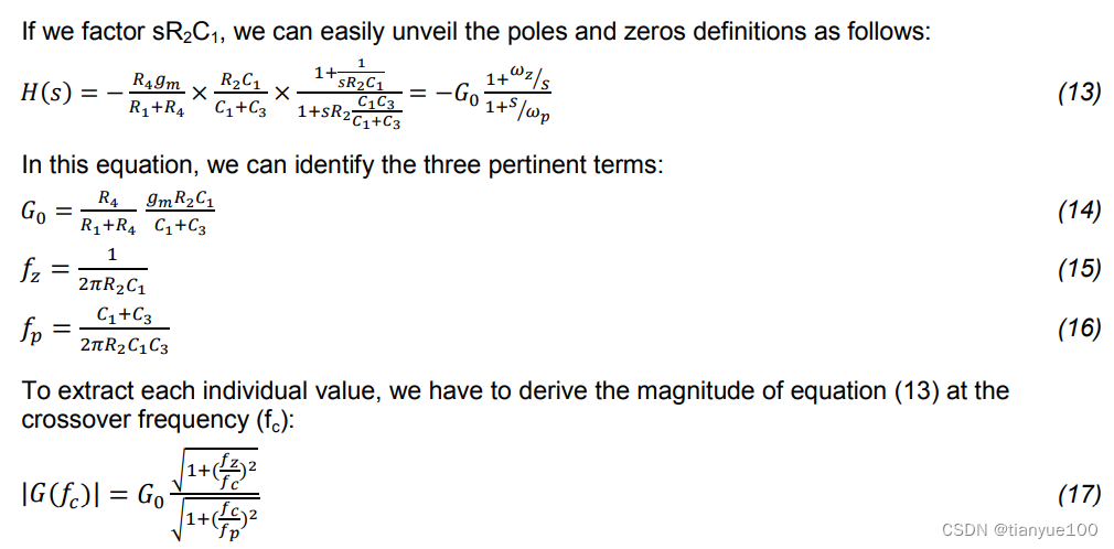
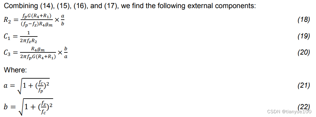
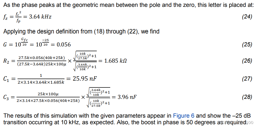
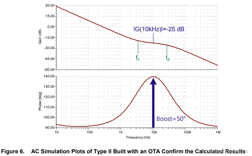
G represents the gain or attenuation you are looking for at the selected crossover frequency (fc). As a design example, if we need a 25 dB attenuation at 10 kHz with a phase boost of 50 degrees, selecting 100 μs transconductance of OTA (also, R1 = 40 kΩ, R4 = 25 kΩ), the external components (R2, C1 and C3) are calculated as follows:

4 Type III Compensator Using Op-Amp
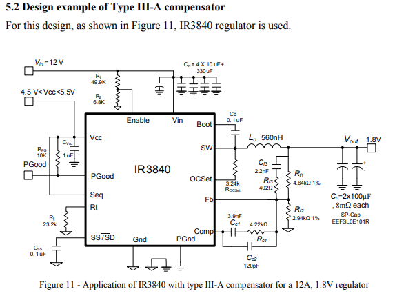
Figure 7 shows the conventional Type III compensation using voltage Op-Amp. There are two poles (fp1 and fp2, besides the pole-at-zero fp0) and two zeros (fz1 and fz2) provided by this compensation. The Type III compensator is used when more than 90 degrees of phase boost are necessary. By adding another pole/zero pair to the Type II compensator, the Type III can theoretically boost the phase up to 180 degrees. The derivation of its transfer function does not really change, which means the principle remains the same with the Type II method.
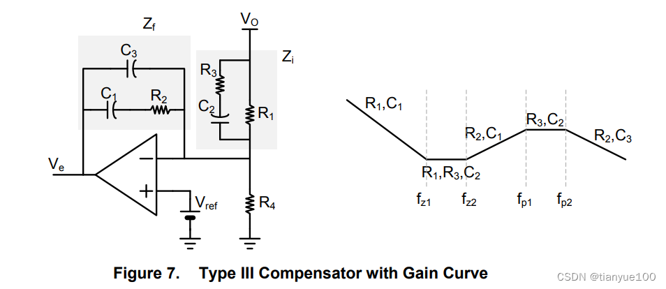
We need to calculate the equivalent impedance Zf placed across the Op-Amp, and divide it by that of Zi to further rearrange the equation:

Note that several of the components involved play a dual role in determining the poles and zeros. So, the calculation can become fairly cumbersome and iterative. But a valid simplifying assumption that can be made is that C1 is much greater than C3. So the locations of the poles and zeros are finally:
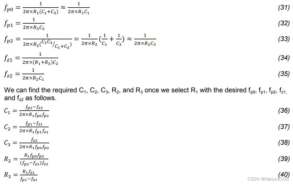
Based on the locations of the poles and zeros, Figure 8 shows a simulation example for the compensator which has an appropriate shape. This compensation scheme adds another RC branch to the Type II compensator. There is an integrator at low frequencies, followed by a pair of zeros. After this, the compensator has a region during where the gain increases with frequency, and the phase during this region is positive. In effect, the compensator is performing the function of a differentiator, measuring the slope of the power supply output waveform.
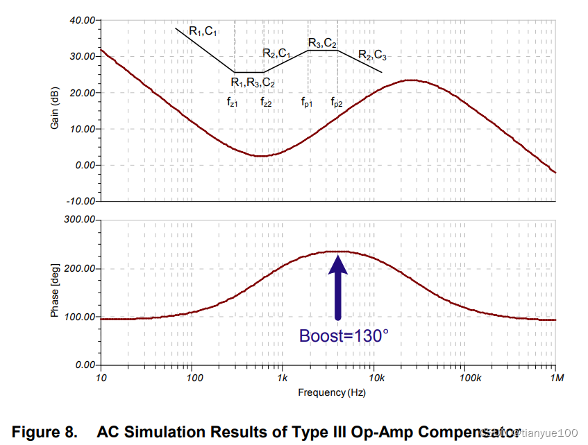
The phase boost in this case is about 130 degrees, but this can be increased by further separation of the poles and zeros. However, you cannot arbitrarily increase this pole-zero separation without considering the detrimental effects on shape of the loop gain. The Type III amplifier is the one for the voltage-mode converters operating in CCM.
5 Type III Compensator Using OTA
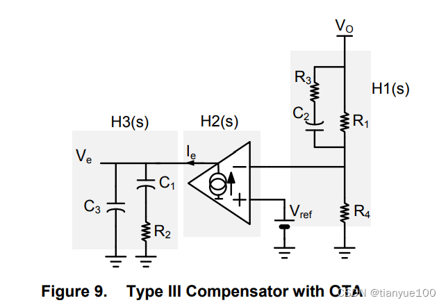
By combining an RC network across the upper resistor R1, it is possible to build a Type III with an OTA. We can also visualize this feedback stage as a product of three cascade transfer functions, H1(s), H2(s), and H3(s) as shown in Figure 9. The transfer function is defined as:
 We know that the output current of the OTA depends on the voltage difference developed between its inputs. In AC, the voltage on the inverting pin depends on the divider network. So, the transfer function we are looking for:

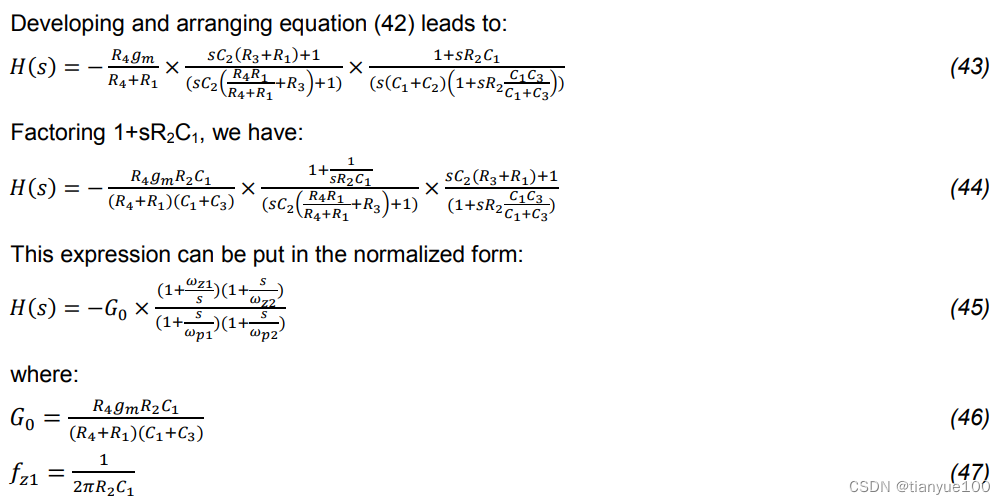

From the values, we need to extract the design expression that will let us calculate the passive values. We first need the magnitude of G at the selected crossover frequency:
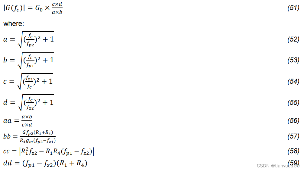

As a design example with a Type III compensator using OTA, if we want to stabilize a 12-V power supply obtained from 2.5-V reference voltage, the ratio between the output voltage and the reference is 12/2.5 = 4.8. To obtain 12-V output, we have R1 equal to 38 kΩ and R4 is 10 kΩ, and the pole (fp1) and zero (fz2) distance cannot be larger than 4.8.
When selecting the crossover frequency, you will have to make sure the maximum phase boost at the selected crossover point is possible (normally it is less than 150 degrees). Let’s assume we want 130 degrees at a 1 kHz crossover frequency, a point where the loop needs 15 dB of amplification.
We can get the first zero and the second pole positions in relationship to the crossover frequency fc:

We know that the distance between the second zero and the first pole has to be less than 4.8 (4.5 is used for safety margin). Positioned in relation to the 1 kHz crossover frequency, they have to be placed at the following positions:

Applying equations from (47) to (59), we find the following values for the passive elements placed around the OTA:
C1 = 14.7 nF, C2 = 9.2 nF, C3 = 113.5 pF, R2 = 123.9 kΩ, R3 = 50 Ω
Once the AC sweep has been performed, the results appear in Figure 10.
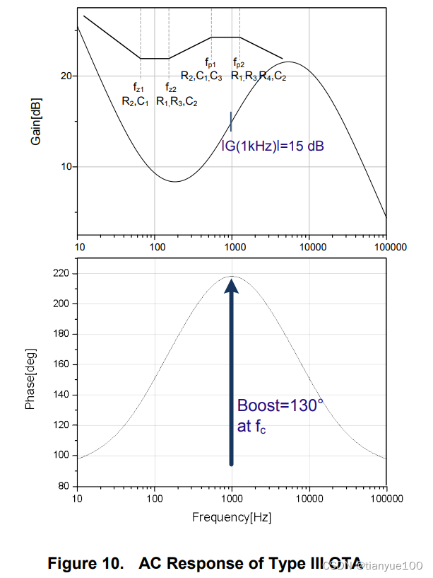
An OTA does not offer the same design flexibility as an Op-Amp. However, IC designers like the structure because of the small semiconductor die size it requires. The lack of virtual ground makes the lower side divider resistor enters the equations and requires attention when deriving poles and zeros placement. Depending on the ratio between the output voltage and the reference voltage, it can hamper the second zero (fz2) and the first pole (fp1) placement in a Type III configuration. This means that if we fix the first pole at some frequency, the location of the second zero is automatically defined. They are not independent. Therefore, there is no great flexibility in using this pole and zero. The phase boost of this type of compensator is needed to offset the sharp phase drop that occurs after the resonant frequency of the power stage.
6 Conclusion
Op-Amp requires local feedback (between its output and inputs) to make it stable and can be wired in a lot of different ways for control loop design. The lower resistor (R4) does not affect the gain-phase plot in Op-Amp applications while the upper resistor (R1) changes the gain-phase results. In adjustable regulators with Op-Amp, it is best to change the lower feedback resistor keeping the upper resistor unchanged if we want to change the output voltage. And also, the error amplifier can be a voltage-to-current amplification device, that is, the gm Op-Amp (Operational Transconductance Amplifier, OTA). This is an open-loop amplifier stage without local feedback. For OTA, both R1 and R4 enter into AC analysis, and note that only the ratio of the feedback resistors is important. Type II compensation scheme adds an RC branch to flatten the gain and improve the phase response in the mid-frequency range. Type II compensators are usually reserved for current-mode control compensation because it cannot be used to improve the phase of the power stage. Type III compensation scheme adds another RC branch to the Type II compensator and is the one to compensate voltage-mode converters operating in CCM. Note that a Type III compensator with an OTA does not offer the same design flexibility compared to the compensator with an Op-Amp because the ratio between the output voltage and the reference voltage can hamper the second zero and the first pole placement.
7 References
1. Practical Feedback Loop Analysis for Voltage-Mode Boost Converter (SLVA633), SW Lee, Texas Instruments, January 2014.
2. Practical Feedback Loop Analysis for Current-Mode Boost Converter (SLVA636), SW Lee, Texas Instruments, March 2014.
最后
以上就是怕孤独草丛最近收集整理的关于Stability Analysis Of Voltage-Feedback Op Amps,Including Compensation Technique2 Development of the Circuit Equations 3 Internal Compensation4 External Compensation, Stability, and Performance5 Dominant-Pole Compensation 6 Gain Compensation 7 Lead Co的全部内容,更多相关Stability内容请搜索靠谱客的其他文章。


![pga是啥oracle,[讨论话题]我的PGA我作主----搞清楚什么是真正的PGA](https://www.shuijiaxian.com/files_image/reation/bcimg11.png)

发表评论 取消回复