我是靠谱客的博主 欣慰西牛,这篇文章主要介绍MATLAB-DSP官方例程------ADC触发PWMMATLAB C2000----- 例程(二)------ADC触发PWM,现在分享给大家,希望可以做个参考。
MATLAB C2000----- 例程(二)------ADC触发PWM
官方例程链接如下:MATLAB
一.模型
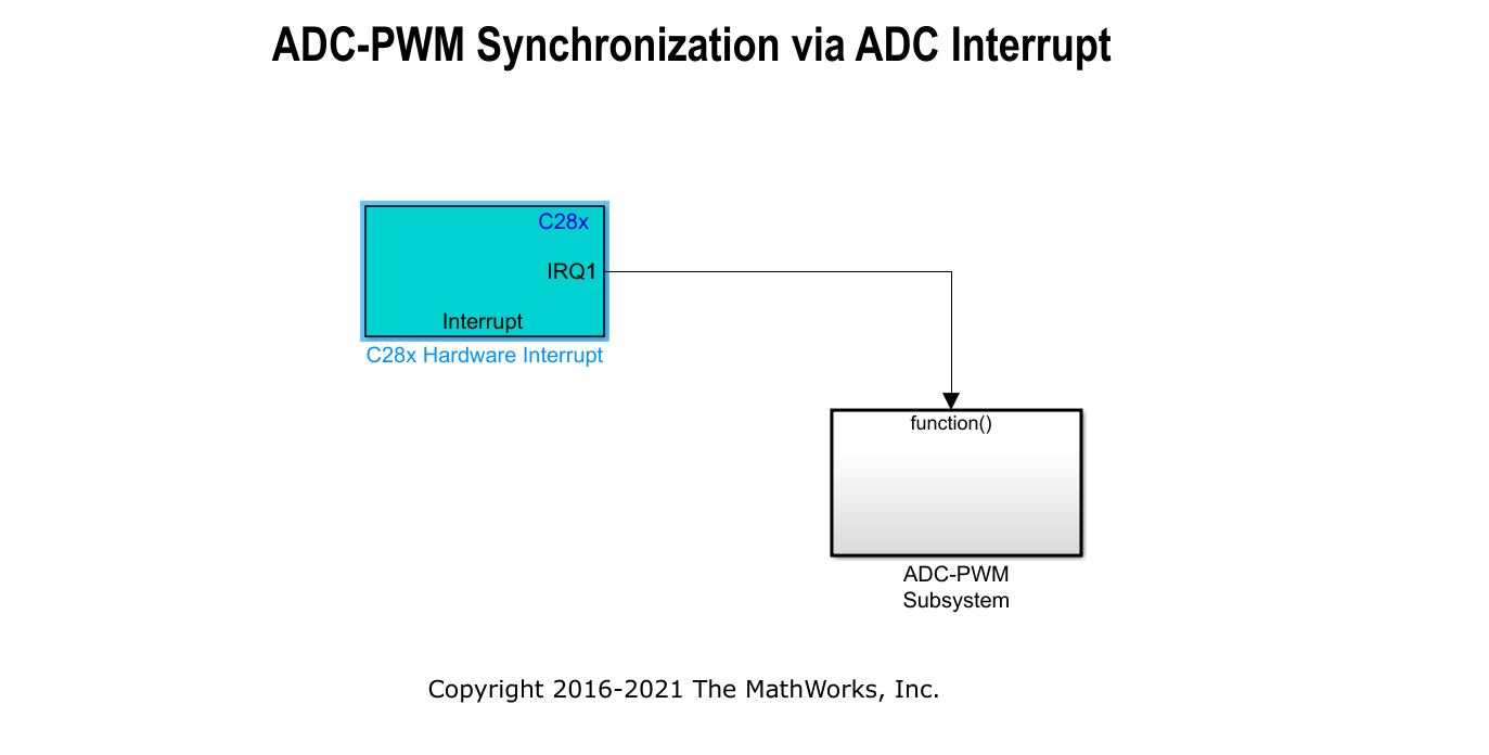
总系统由两哥子系统组成一个中断触发 一个ADC-PWM
ADC-PWM系统
![[外链图片转存失败,源站可能有防盗链机制,建议将图片保存下来直接上传(img-3IptgCAh-1628340766621)(C:My_Project_MarkdownStudy_YellowNewimageADCPWM1.png)]](https://www.shuijiaxian.com/files_image/2023060717/39d80796f1ef4e599ff31cda58456408.png)
ADC触发pwm并且adc的输出为pwm的duty的输入,且为五倍关系。
二.烧入过程
与上篇文章相似
三.代码分析
我们先看一下所生成的文件
![[外链图片转存失败,源站可能有防盗链机制,建议将图片保存下来直接上传(img-rfSXnio6-1628340766624)(C:My_Project_MarkdownStudy_YellowNewimageADCPWM3.png)]](https://www.shuijiaxian.com/files_image/2023060717/f11ff9a6edca42109755f2d700955243.png)
如红框所示 这些为所生成的文件
-
c2807x_2837xx_adcpwmasynctest_ert_data.c
主要定义了数据的大小
-
c2807x_2837xx_adcpwmasynctest_ert.c
初始化PWM和ADC 以及模型所使用的函数以及结构体
-
c2837xDBoard_Realtime_Support.c
一些常用型的库函数
-
c2837xDSchedulerTimer0.c
就是跟求解器步长相关的函数,如果加入积分模块很有可能就在这里运算。
-
ert_main.c
主函数
初始化外设
-
MW_c28xGlobalInterrupts.c
-
MW_c28xGPIO.c
-
MW_c28xx_adc.c
-
MW_c28xx_board.c
-
MW_c28xx_csl.c
-
MW_c28xx_pwm.c
-
MW_c28xx_xbar.c
-
profiler_Support.c // 可能为调试文件暂未尝试 (看大佬这样说的)
ert_main.c
/*
 * File: ert_main.c
 *
 * Code generated for Simulink model 'c2807x_2837xx_adcpwmasynctest_ert'.
 *
 * Model version                  : 9.1
 * Simulink Coder version         : 9.5 (R2021a) 14-Nov-2020
 * C/C++ source code generated on : Fri Aug  6 09:56:42 2021
 *
 * Target selection: ert.tlc
 * Embedded hardware selection: Texas Instruments->C2000
 * Code generation objectives: Unspecified
 * Validation result: Not run
 */

#include "c2807x_2837xx_adcpwmasynctest_ert.h"
#include "rtwtypes.h"

volatile int IsrOverrun = 0;
static boolean_T OverrunFlag = 0;
void rt_OneStep(void)
{
}

volatile boolean_T stopRequested;
volatile boolean_T runModel;
int main(void)
{
  float modelBaseRate = 0.2; //进入中断时间 0.2秒进入一次中断
  float systemClock = 200;  //CPU晶振频率,与Clocking中的参数相互对应

  /* Initialize variables */
  stopRequested = false;
  runModel = false;
  c2000_flash_init();
  init_board();

#ifdef MW_EXEC_PROFILER_ON

  config_profilerTimer();

#endif

  ;
  rtmSetErrorStatus(c2807x_2837xx_adcpwmasynctes_M, 0); //_M结构体的错误标志为0
  c2807x_2837xx_adcpwmasynctest_ert_initialize(); //初始化
  globalInterruptDisable();
  configureTimer0(modelBaseRate, systemClock); // 初始化定时器计数时间
  runModel =
    rtmGetErrorStatus(c2807x_2837xx_adcpwmasynctes_M) == (NULL);
  enableTimer0Interrupt();
  enable_interrupts();
  globalInterruptEnable();
  while (runModel) {
    stopRequested = !(
                      rtmGetErrorStatus(c2807x_2837xx_adcpwmasynctes_M) == (NULL));
  } //判断 stopRequested 不等于_M结构体的错误标志指向空指针

  /* Disable rt_OneStep() here */

  /* Terminate model */
  c2807x_2837xx_adcpwmasynctest_ert_terminate();
  globalInterruptDisable();
  return 0;
}

/*
 * File trailer for generated code.
 *
 * [EOF]
 */
c2807x_2837xx_adcpwmasynctest_ert.c
/*
 * File: c2807x_2837xx_adcpwmasynctest_ert.c
 *
 * Code generated for Simulink model 'c2807x_2837xx_adcpwmasynctest_ert'.
 *
 * Model version                  : 9.1
 * Simulink Coder version         : 9.5 (R2021a) 14-Nov-2020
 * C/C++ source code generated on : Fri Aug  6 09:56:42 2021
 *
 * Target selection: ert.tlc
 * Embedded hardware selection: Texas Instruments->C2000
 * Code generation objectives: Unspecified
 * Validation result: Not run
 */

#include "c2807x_2837xx_adcpwmasynctest_ert.h"
#include "c2807x_2837xx_adcpwmasynctest_ert_private.h"

/* Block signals (default storage) */
B_c2807x_2837xx_adcpwmasyncte_T c2807x_2837xx_adcpwmasynctest_B;

/* Real-time model */
static RT_MODEL_c2807x_2837xx_adcpwm_T c2807x_2837xx_adcpwmasynctes_M_;
RT_MODEL_c2807x_2837xx_adcpwm_T *const c2807x_2837xx_adcpwmasynctes_M =
  &c2807x_2837xx_adcpwmasynctes_M_;
uint16_T MW_adcAInitFlag = 0;

/* Hardware Interrupt Block: '<Root>/C28x Hardware Interrupt' */
//中断函数
void isr_int1pie1_task_fcn(void)
{
  if (1 == runModel) {
    /* Call the system: <Root>/ADC-PWM Subsystem */
    {
      /* S-Function (c28xisr_c2000): '<Root>/C28x Hardware Interrupt' */

      /* Output and update for function-call system: '<Root>/ADC-PWM Subsystem' */
      {
        uint16_T rtb_Gain;

        /* S-Function (c2802xadc): '<S1>/ADC' */
        {
          /*  Internal Reference Voltage : Fixed scale 0 to 3.3 V range.  */
          /*  External Reference Voltage : Allowable ranges of VREFHI(ADCINA0) = 3.3 and VREFLO(tied to ground) = 0  */
          c2807x_2837xx_adcpwmasynctest_B.ADC = (AdcaResultRegs.ADCRESULT0);
        }

        /* Gain: '<S1>/Gain' */
        rtb_Gain = (uint16_T)(((uint32_T)
          c2807x_2837xx_adcpwmasynctest_P.Gain_Gain *
          c2807x_2837xx_adcpwmasynctest_B.ADC) >> 13U);  // (40950>>13)*ADC采样结果 = 5*ADC_result

        /* S-Function (c2802xpwm): '<S1>/ePWM' */

        /*-- Update CMPA value for ePWM1 --*/
        {
          EPwm1Regs.CMPA.bit.CMPA = (uint16_T)(rtb_Gain);  //赋值给结果寄存器
        }
      }

      /* End of Outputs for S-Function (c28xisr_c2000): '<Root>/C28x Hardware Interrupt' */
    }
  }
}

/* Model step function */
void c2807x_2837xx_adcpwmasynctest_ert_step(void)
{
  /* (no output/update code required) */
}

/* Model initialize function */
void c2807x_2837xx_adcpwmasynctest_ert_initialize(void)
{
  /* Registration code */

  /* initialize error status */
  rtmSetErrorStatus(c2807x_2837xx_adcpwmasynctes_M, (NULL));

  /* block I/O */
  (void) memset(((void *) &c2807x_2837xx_adcpwmasynctest_B), 0,
                sizeof(B_c2807x_2837xx_adcpwmasyncte_T)); //给结构体赋值为0

  /* SystemInitialize for S-Function (c28xisr_c2000): '<Root>/C28x Hardware Interrupt' incorporates:
   *  SubSystem: '<Root>/ADC-PWM Subsystem'
   */

  /* System initialize for function-call system: '<Root>/ADC-PWM Subsystem' */

  /* Start for S-Function (c2802xadc): '<S1>/ADC' */
  if (MW_adcAInitFlag == 0) {
    InitAdcA();
    MW_adcAInitFlag = 1;
  } // 利用控制位只初始化ADC一次

  config_ADCA_SOC0 ();

  /* Start for S-Function (c2802xpwm): '<S1>/ePWM' */

  /*** Initialize ePWM1 modules ***/
  {
    /*  // Time Base Control Register
       EPwm1Regs.TBCTL.bit.CTRMODE              = 2;          // Counter Mode
       EPwm1Regs.TBCTL.bit.SYNCOSEL             = 3;          // Sync Output Select
       EPwm1Regs.TBCTL2.bit.SYNCOSELX           = 0;          // Sync Output Select - additional options

       EPwm1Regs.TBCTL.bit.PRDLD                = 0;          // Shadow select

       EPwm1Regs.TBCTL2.bit.PRDLDSYNC           = 0;          // Shadow select

       EPwm1Regs.TBCTL.bit.PHSEN                = 0;          // Phase Load Enable
       EPwm1Regs.TBCTL.bit.PHSDIR               = 0;          // Phase Direction Bit
       EPwm1Regs.TBCTL.bit.HSPCLKDIV            = 0;          // High Speed TBCLK Pre-scaler
       EPwm1Regs.TBCTL.bit.CLKDIV               = 0;          // Time Base Clock Pre-scaler
       EPwm1Regs.TBCTL.bit.SWFSYNC              = 0;          // Software Force Sync Pulse
     */
    EPwm1Regs.TBCTL.all = (EPwm1Regs.TBCTL.all & ~0x3FFF) | 0x32;
    EPwm1Regs.TBCTL2.all = (EPwm1Regs.TBCTL2.all & ~0xF000) | 0x0;

    /*-- Setup Time-Base (TB) Submodule --*/
    EPwm1Regs.TBPRD = 20480;           // Time Base Period Register

    /* // Time-Base Phase Register
       EPwm1Regs.TBPHS.bit.TBPHS               = 0;          // Phase offset register
     */
    EPwm1Regs.TBPHS.all = (EPwm1Regs.TBPHS.all & ~0xFFFF0000) | 0x0;

    // Time Base Counter Register
    EPwm1Regs.TBCTR = 0x0000;          /* Clear counter*/

    /*-- Setup Counter_Compare (CC) Submodule --*/
    /*	// Counter Compare Control Register

       EPwm1Regs.CMPCTL.bit.LOADASYNC           = 0U;          // Active Compare A Load SYNC Option
       EPwm1Regs.CMPCTL.bit.LOADBSYNC           = 0U;          // Active Compare B Load SYNC Option
       EPwm1Regs.CMPCTL.bit.LOADAMODE           = 0U;          // Active Compare A Load
       EPwm1Regs.CMPCTL.bit.LOADBMODE           = 0U;          // Active Compare B Load
       EPwm1Regs.CMPCTL.bit.SHDWAMODE           = 0;          // Compare A Register Block Operating Mode
       EPwm1Regs.CMPCTL.bit.SHDWBMODE           = 0;          // Compare B Register Block Operating Mode
     */
    EPwm1Regs.CMPCTL.all = (EPwm1Regs.CMPCTL.all & ~0x3C5F) | 0x0;

    /* EPwm1Regs.CMPCTL2.bit.SHDWCMODE           = 0;          // Compare C Register Block Operating Mode
       EPwm1Regs.CMPCTL2.bit.SHDWDMODE           = 0;          // Compare D Register Block Operating Mode
       EPwm1Regs.CMPCTL2.bit.LOADCSYNC           = 0U;          // Active Compare C Load SYNC Option
       EPwm1Regs.CMPCTL2.bit.LOADDSYNC           = 0U;          // Active Compare D Load SYNC Option
       EPwm1Regs.CMPCTL2.bit.LOADCMODE           = 0U;          // Active Compare C Load
       EPwm1Regs.CMPCTL2.bit.LOADDMODE           = 0U;          // Active Compare D Load
     */
    EPwm1Regs.CMPCTL2.all = (EPwm1Regs.CMPCTL2.all & ~0x3C5F) | 0x0;
    EPwm1Regs.CMPA.bit.CMPA = 5000;    // Counter Compare A Register
    EPwm1Regs.CMPB.bit.CMPB = 0;       // Counter Compare B Register
    EPwm1Regs.CMPC = 0;                // Counter Compare C Register
    EPwm1Regs.CMPD = 0;                // Counter Compare D Register

    /*-- Setup Action-Qualifier (AQ) Submodule --*/
    EPwm1Regs.AQCTLA.all = 96; // Action Qualifier Control Register For Output A
    EPwm1Regs.AQCTLB.all = 0;  // Action Qualifier Control Register For Output B

    /*	// Action Qualifier Software Force Register
       EPwm1Regs.AQSFRC.bit.RLDCSF              = 0;          // Reload from Shadow Options
     */
    EPwm1Regs.AQSFRC.all = (EPwm1Regs.AQSFRC.all & ~0xC0) | 0x0;

    /*	// Action Qualifier Continuous S/W Force Register
       EPwm1Regs.AQCSFRC.bit.CSFA               = 0;          // Continuous Software Force on output A
       EPwm1Regs.AQCSFRC.bit.CSFB               = 0;          // Continuous Software Force on output B
     */
    EPwm1Regs.AQCSFRC.all = (EPwm1Regs.AQCSFRC.all & ~0xF) | 0x0;

    /*-- Setup Dead-Band Generator (DB) Submodule --*/
    /*	// Dead-Band Generator Control Register
       EPwm1Regs.DBCTL.bit.OUT_MODE             = 0;          // Dead Band Output Mode Control
       EPwm1Regs.DBCTL.bit.IN_MODE              = 0;          // Dead Band Input Select Mode Control
       EPwm1Regs.DBCTL.bit.POLSEL               = 0;          // Polarity Select Control
       EPwm1Regs.DBCTL.bit.HALFCYCLE            = 0;          // Half Cycle Clocking Enable
       EPwm1Regs.DBCTL.bit.SHDWDBREDMODE        = 0;          // DBRED shadow mode
       EPwm1Regs.DBCTL.bit.SHDWDBFEDMODE        = 0;          // DBFED shadow mode
       EPwm1Regs.DBCTL.bit.LOADREDMODE          = 4U;        // DBRED load
       EPwm1Regs.DBCTL.bit.LOADFEDMODE          = 4U;        // DBFED load
     */
    EPwm1Regs.DBCTL.all = (EPwm1Regs.DBCTL.all & ~0x8FFF) | 0x0;
    EPwm1Regs.DBRED.bit.DBRED = (uint16_T)(0);
                         // Dead-Band Generator Rising Edge Delay Count Register
    EPwm1Regs.DBFED.bit.DBFED = (uint16_T)(0);
                        // Dead-Band Generator Falling Edge Delay Count Register

    /*-- Setup Event-Trigger (ET) Submodule --*/
    /*	// Event Trigger Selection and Pre-Scale Register
       EPwm1Regs.ETSEL.bit.SOCAEN               = 1;          // Start of Conversion A Enable
       EPwm1Regs.ETSEL.bit.SOCASELCMP           = 0;
       EPwm1Regs.ETSEL.bit.SOCASEL              = 2;          // Start of Conversion A Select
       EPwm1Regs.ETPS.bit.SOCPSSEL              = 1;          // EPWM1SOC Period Select
       EPwm1Regs.ETSOCPS.bit.SOCAPRD2           = 1;
       EPwm1Regs.ETSEL.bit.SOCBEN               = 0;          // Start of Conversion B Enable
       EPwm1Regs.ETSEL.bit.SOCBSELCMP           = 0;
       EPwm1Regs.ETSEL.bit.SOCBSEL              = 1;          // Start of Conversion A Select
       EPwm1Regs.ETPS.bit.SOCPSSEL              = 1;          // EPWM1SOCB Period Select
       EPwm1Regs.ETSOCPS.bit.SOCBPRD2           = 1;
       EPwm1Regs.ETSEL.bit.INTEN                = 0;          // EPWM1INTn Enable
       EPwm1Regs.ETSEL.bit.INTSELCMP            = 0;
       EPwm1Regs.ETSEL.bit.INTSEL               = 1;          // Start of Conversion A Select
       EPwm1Regs.ETPS.bit.INTPSSEL              = 1;          // EPWM1INTn Period Select
       EPwm1Regs.ETINTPS.bit.INTPRD2            = 1;
     */
    EPwm1Regs.ETSEL.all = (EPwm1Regs.ETSEL.all & ~0xFF7F) | 0x1A01;
    EPwm1Regs.ETPS.all = (EPwm1Regs.ETPS.all & ~0x30) | 0x30;
    EPwm1Regs.ETSOCPS.all = (EPwm1Regs.ETSOCPS.all & ~0xF0F) | 0x101;
    EPwm1Regs.ETINTPS.all = (EPwm1Regs.ETINTPS.all & ~0xF) | 0x1;

    /*-- Setup PWM-Chopper (PC) Submodule --*/
    /*	// PWM Chopper Control Register
       EPwm1Regs.PCCTL.bit.CHPEN                = 0;          // PWM chopping enable
       EPwm1Regs.PCCTL.bit.CHPFREQ              = 0;          // Chopping clock frequency
       EPwm1Regs.PCCTL.bit.OSHTWTH              = 0;          // One-shot pulse width
       EPwm1Regs.PCCTL.bit.CHPDUTY              = 0;          // Chopping clock Duty cycle
     */
    EPwm1Regs.PCCTL.all = (EPwm1Regs.PCCTL.all & ~0x7FF) | 0x0;

    /*-- Set up Trip-Zone (TZ) Submodule --*/
    EALLOW;
    EPwm1Regs.TZSEL.all = 0;           // Trip Zone Select Register

    /*	// Trip Zone Control Register
       EPwm1Regs.TZCTL.bit.TZA                  = 3;          // TZ1 to TZ6 Trip Action On EPWM1A
       EPwm1Regs.TZCTL.bit.TZB                  = 3;          // TZ1 to TZ6 Trip Action On EPWM1B
       EPwm1Regs.TZCTL.bit.DCAEVT1              = 3;          // EPWM1A action on DCAEVT1
       EPwm1Regs.TZCTL.bit.DCAEVT2              = 3;          // EPWM1A action on DCAEVT2
       EPwm1Regs.TZCTL.bit.DCBEVT1              = 3;          // EPWM1B action on DCBEVT1
       EPwm1Regs.TZCTL.bit.DCBEVT2              = 3;          // EPWM1B action on DCBEVT2
     */
    EPwm1Regs.TZCTL.all = (EPwm1Regs.TZCTL.all & ~0xFFF) | 0xFFF;

    /*	// Trip Zone Enable Interrupt Register
       EPwm1Regs.TZEINT.bit.OST                 = 0;          // Trip Zones One Shot Int Enable
       EPwm1Regs.TZEINT.bit.CBC                 = 0;          // Trip Zones Cycle By Cycle Int Enable
       EPwm1Regs.TZEINT.bit.DCAEVT1             = 0;          // Digital Compare A Event 1 Int Enable
       EPwm1Regs.TZEINT.bit.DCAEVT2             = 0;          // Digital Compare A Event 2 Int Enable
       EPwm1Regs.TZEINT.bit.DCBEVT1             = 0;          // Digital Compare B Event 1 Int Enable
       EPwm1Regs.TZEINT.bit.DCBEVT2             = 0;          // Digital Compare B Event 2 Int Enable
     */
    EPwm1Regs.TZEINT.all = (EPwm1Regs.TZEINT.all & ~0x7E) | 0x0;

    /*	// Digital Compare A Control Register
       EPwm1Regs.DCACTL.bit.EVT1SYNCE           = 0;          // DCAEVT1 SYNC Enable
       EPwm1Regs.DCACTL.bit.EVT1SOCE            = 1;          // DCAEVT1 SOC Enable
       EPwm1Regs.DCACTL.bit.EVT1FRCSYNCSEL      = 0;          // DCAEVT1 Force Sync Signal
       EPwm1Regs.DCACTL.bit.EVT1SRCSEL          = 0;          // DCAEVT1 Source Signal
       EPwm1Regs.DCACTL.bit.EVT2FRCSYNCSEL      = 0;          // DCAEVT2 Force Sync Signal
       EPwm1Regs.DCACTL.bit.EVT2SRCSEL          = 0;          // DCAEVT2 Source Signal
     */
    EPwm1Regs.DCACTL.all = (EPwm1Regs.DCACTL.all & ~0x30F) | 0x4;

    /*	// Digital Compare B Control Register
       EPwm1Regs.DCBCTL.bit.EVT1SYNCE           = 0;          // DCBEVT1 SYNC Enable
       EPwm1Regs.DCBCTL.bit.EVT1SOCE            = 0;          // DCBEVT1 SOC Enable
       EPwm1Regs.DCBCTL.bit.EVT1FRCSYNCSEL      = 0;          // DCBEVT1 Force Sync Signal
       EPwm1Regs.DCBCTL.bit.EVT1SRCSEL          = 0;          // DCBEVT1 Source Signal
       EPwm1Regs.DCBCTL.bit.EVT2FRCSYNCSEL      = 0;          // DCBEVT2 Force Sync Signal
       EPwm1Regs.DCBCTL.bit.EVT2SRCSEL          = 0;          // DCBEVT2 Source Signal
     */
    EPwm1Regs.DCBCTL.all = (EPwm1Regs.DCBCTL.all & ~0x30F) | 0x0;

    /*	// Digital Compare Trip Select Register
       EPwm1Regs.DCTRIPSEL.bit.DCAHCOMPSEL      = 0;          // Digital Compare A High COMP Input Select

       EPwm1Regs.DCTRIPSEL.bit.DCALCOMPSEL      = 1;          // Digital Compare A Low COMP Input Select
       EPwm1Regs.DCTRIPSEL.bit.DCBHCOMPSEL      = 0;          // Digital Compare B High COMP Input Select
       EPwm1Regs.DCTRIPSEL.bit.DCBLCOMPSEL      = 1;          // Digital Compare B Low COMP Input Select

     */
    EPwm1Regs.DCTRIPSEL.all = (EPwm1Regs.DCTRIPSEL.all & ~ 0xFFFF) | 0x1010;

    /*	// Trip Zone Digital Comparator Select Register
       EPwm1Regs.TZDCSEL.bit.DCAEVT1            = 0;          // Digital Compare Output A Event 1
       EPwm1Regs.TZDCSEL.bit.DCAEVT2            = 0;          // Digital Compare Output A Event 2
       EPwm1Regs.TZDCSEL.bit.DCBEVT1            = 0;          // Digital Compare Output B Event 1
       EPwm1Regs.TZDCSEL.bit.DCBEVT2            = 0;          // Digital Compare Output B Event 2
     */
    EPwm1Regs.TZDCSEL.all = (EPwm1Regs.TZDCSEL.all & ~0xFFF) | 0x0;

    /*	// Digital Compare Filter Control Register
       EPwm1Regs.DCFCTL.bit.BLANKE              = 0;          // Blanking Enable/Disable
       EPwm1Regs.DCFCTL.bit.PULSESEL            = 1;          // Pulse Select for Blanking & Capture Alignment
       EPwm1Regs.DCFCTL.bit.BLANKINV            = 0;          // Blanking Window Inversion
       EPwm1Regs.DCFCTL.bit.SRCSEL              = 0;          // Filter Block Signal Source Select
     */
    EPwm1Regs.DCFCTL.all = (EPwm1Regs.DCFCTL.all & ~0x3F) | 0x10;
    EPwm1Regs.DCFOFFSET = 0;           // Digital Compare Filter Offset Register
    EPwm1Regs.DCFWINDOW = 0;           // Digital Compare Filter Window Register

    /*	// Digital Compare Capture Control Register
       EPwm1Regs.DCCAPCTL.bit.CAPE              = 0;          // Counter Capture Enable
     */
    EPwm1Regs.DCCAPCTL.all = (EPwm1Regs.DCCAPCTL.all & ~0x1) | 0x0;

    /*	// HRPWM Configuration Register
       EPwm1Regs.HRCNFG.bit.SWAPAB              = 0;          // Swap EPWMA and EPWMB Outputs Bit
       EPwm1Regs.HRCNFG.bit.SELOUTB             = 0;          // EPWMB Output Selection Bit
     */
    EPwm1Regs.HRCNFG.all = (EPwm1Regs.HRCNFG.all & ~0xA0) | 0x0;

    /* Update the Link Registers with the link value for all the Compare values and TBPRD */
    /* No error is thrown if the ePWM register exists in the model or not */
    EPwm1Regs.EPWMXLINK.bit.TBPRDLINK = 0;
    EPwm1Regs.EPWMXLINK.bit.CMPALINK = 0;
    EPwm1Regs.EPWMXLINK.bit.CMPBLINK = 0;
    EPwm1Regs.EPWMXLINK.bit.CMPCLINK = 0;
    EPwm1Regs.EPWMXLINK.bit.CMPDLINK = 0;

    /* SYNCPER - Peripheral synchronization output event
       EPwm1Regs.HRPCTL.bit.PWMSYNCSEL            = 0;          // EPWMSYNCPER selection
       EPwm1Regs.HRPCTL.bit.PWMSYNCSELX           = 0;          //  EPWMSYNCPER selection
     */
    EPwm1Regs.HRPCTL.all = (EPwm1Regs.HRPCTL.all & ~0x72) | 0x0;
    EDIS;
    EALLOW;

    /* Enable TBCLK within the EPWM*/
    CpuSysRegs.PCLKCR0.bit.TBCLKSYNC = 1;
    EDIS;
  }

  /* End of SystemInitialize for S-Function (c28xisr_c2000): '<Root>/C28x Hardware Interrupt' */
}

/* Model terminate function */
void c2807x_2837xx_adcpwmasynctest_ert_terminate(void)
{
  /* (no terminate code required) */
}

/*
 * File trailer for generated code.
 *
 * [EOF]
 */
c2837xDSchedulerTimer0.c
/* Copyright 2015-2020 The MathWorks, Inc. */

#include "F2837xD_device.h"
#include "F2837xD_cputimer.h"
#include "F2837xD_cputimervars.h"
#include "MW_c28xx_pie.h"
#include "F2837xD_Ipc_drivers.h"

extern void rt_OneStep(void);
#define CPU01_TO_CPU02_PASSMSG  0x0003FFF4
extern uint32_t mwInitStart;
extern uint32_t mwInitEnd;

interrupt void TINT0_isr(void)
{
      #ifdef PIEMASK0
        volatile unsigned int PIEIER1_stack_save = PieCtrlRegs.PIEIER1.all;
      #endif
      #ifdef PIEMASK1
        volatile unsigned int PIEIER2_stack_save  = PieCtrlRegs.PIEIER2.all;
      #endif
      #ifdef PIEMASK2
        volatile unsigned int PIEIER3_stack_save  = PieCtrlRegs.PIEIER3.all;
      #endif
      #ifdef PIEMASK3
        volatile unsigned int PIEIER4_stack_save  = PieCtrlRegs.PIEIER4.all;
      #endif
      #ifdef PIEMASK4
        volatile unsigned int PIEIER5_stack_save  = PieCtrlRegs.PIEIER5.all;
      #endif
      #ifdef PIEMASK5
        volatile unsigned int PIEIER6_stack_save  = PieCtrlRegs.PIEIER6.all;
      #endif
      #ifdef PIEMASK6
        volatile unsigned int PIEIER7_stack_save  = PieCtrlRegs.PIEIER7.all;
      #endif
      #ifdef PIEMASK7
        volatile unsigned int PIEIER8_stack_save  = PieCtrlRegs.PIEIER8.all;
      #endif
      #ifdef PIEMASK8
        volatile unsigned int PIEIER9_stack_save  = PieCtrlRegs.PIEIER9.all;
      #endif
      #ifdef PIEMASK9
        volatile unsigned int PIEIER10_stack_save = PieCtrlRegs.PIEIER10.all;
      #endif
      #ifdef PIEMASK10
        volatile unsigned int PIEIER11_stack_save = PieCtrlRegs.PIEIER11.all;
      #endif
      #ifdef PIEMASK11
        volatile unsigned int PIEIER12_stack_save = PieCtrlRegs.PIEIER12.all;
      #endif

      #ifdef PIEMASK0
        PieCtrlRegs.PIEIER1.all &= ~PIEMASK0;      /* disable group1 lower/equal priority interrupts */
      #endif
      #ifdef PIEMASK1
        PieCtrlRegs.PIEIER2.all &= ~PIEMASK1;      /* disable group2 lower/equal priority interrupts */
      #endif
      #ifdef PIEMASK2
        PieCtrlRegs.PIEIER3.all &= ~PIEMASK2;      /* disable group3 lower/equal priority interrupts */
      #endif
      #ifdef PIEMASK3
        PieCtrlRegs.PIEIER4.all &= ~PIEMASK3;      /* disable group4 lower/equal priority interrupts */
      #endif
      #ifdef PIEMASK4
        PieCtrlRegs.PIEIER5.all &= ~PIEMASK4;      /* disable group5 lower/equal priority interrupts */
      #endif
      #ifdef PIEMASK5
        PieCtrlRegs.PIEIER6.all &= ~PIEMASK5;      /* disable group6 lower/equal priority interrupts */
      #endif
      #ifdef PIEMASK6
        PieCtrlRegs.PIEIER7.all &= ~PIEMASK6;      /* disable group7 lower/equal priority interrupts */
      #endif
      #ifdef PIEMASK7
        PieCtrlRegs.PIEIER8.all &= ~PIEMASK7;      /* disable group8 lower/equal priority interrupts */
      #endif
      #ifdef PIEMASK8
        PieCtrlRegs.PIEIER9.all &= ~PIEMASK8;      /* disable group9 lower/equal priority interrupts */
      #endif
      #ifdef PIEMASK9
        PieCtrlRegs.PIEIER10.all &= ~PIEMASK9;     /* disable group10 lower/equal priority interrupts */
      #endif
      #ifdef PIEMASK10
        PieCtrlRegs.PIEIER11.all &= ~PIEMASK10;    /* disable group11 lower/equal priority interrupts */
      #endif
      #ifdef PIEMASK11
        PieCtrlRegs.PIEIER12.all &= ~PIEMASK11;    /* disable group12 lower/equal priority interrupts */
      #endif
	  #ifdef PIEMASK12
		IER &= ~(M_INT13);
      #endif
	  #ifdef PIEMASK13
		IER &= ~(M_INT14);
      #endif

      asm(" RPT #5 || NOP");               /* wait 5 cycles */ //等待五个周期
      IFR &= ~IFRMASK;                            /* eventually disable lower/equal priority pending interrupts */
      PieCtrlRegs.PIEACK.all = IFRMASK;          /* ACK to allow other interrupts from the same group to fire */
      IER |= 1;
      EINT;                                /* global interrupt enable */
      rt_OneStep();
      DINT;                                /* disable global interrupts during context switch, CPU will enable global interrupts after exiting ISR */
      #ifdef PIEMASK0
        PieCtrlRegs.PIEIER1.all = PIEIER1_stack_save;/*restore PIEIER register that was modified */
      #endif
      #ifdef PIEMASK1
        PieCtrlRegs.PIEIER2.all = PIEIER2_stack_save;/*restore PIEIER register that was modified */
      #endif
      #ifdef PIEMASK2
        PieCtrlRegs.PIEIER3.all = PIEIER3_stack_save;/*restore PIEIER register that was modified */
      #endif
      #ifdef PIEMASK3
        PieCtrlRegs.PIEIER4.all = PIEIER4_stack_save;/*restore PIEIER register that was modified */
      #endif
      #ifdef PIEMASK4
        PieCtrlRegs.PIEIER5.all = PIEIER5_stack_save;/*restore PIEIER register that was modified */
      #endif
      #ifdef PIEMASK5
        PieCtrlRegs.PIEIER6.all = PIEIER6_stack_save;/*restore PIEIER register that was modified */
      #endif
      #ifdef PIEMASK6
        PieCtrlRegs.PIEIER7.all = PIEIER7_stack_save;/*restore PIEIER register that was modified */
      #endif
      #ifdef PIEMASK7
        PieCtrlRegs.PIEIER8.all = PIEIER8_stack_save;/*restore PIEIER register that was modified */
      #endif
      #ifdef PIEMASK8
        PieCtrlRegs.PIEIER9.all = PIEIER9_stack_save;/*restore PIEIER register that was modified */
      #endif
      #ifdef PIEMASK9
        PieCtrlRegs.PIEIER10.all= PIEIER10_stack_save;/*restore PIEIER register that was modified */
      #endif
      #ifdef PIEMASK10
        PieCtrlRegs.PIEIER11.all= PIEIER11_stack_save;/*restore PIEIER register that was modified */
      #endif
      #ifdef PIEMASK11
        PieCtrlRegs.PIEIER12.all= PIEIER12_stack_save;/*restore PIEIER register that was modified */
      #endif
	  #ifdef PIEMASK12
		IER |= M_INT13;
      #endif
	  #ifdef PIEMASK13
		IER |= M_INT14;
      #endif
}

void configureTimer0(float baseRate, float systemClock)
{
  #ifndef TIC2000_SOC_BASEPRODUCT
    #ifdef CPU1
        EINT;
        uint32_t ipcCountVar = 0;
        if (0x425 == mwInitStart)
        {
            /* Wait until completion of CPU2 GPIO initialization */
            while ((0x36E != mwInitEnd))
            {
                ipcCountVar++;
            }
        }
        DINT;
    #else
	      uint32_t *pulMsgRam;
	      pulMsgRam = (void *)CPU01_TO_CPU02_PASSMSG;
        IPCLiteLtoRDataWrite(IPC_FLAG0, pulMsgRam[2], 0x36E,
                         IPC_LENGTH_32_BITS, IPC_FLAG31);
    #endif
  #endif

    /* InitCpuTimers() - CPU Timers are initialized in
     * MW_c28xx_board.c in the generated code.
     */

	/* Configure CPU-Timer 0 to interrupt every base rate. */
	/* Parameters:  Timer Pointer, CPU Freq in MHz, Period in usec. */
	ConfigCpuTimer(&CpuTimer0, systemClock, baseRate * 1000000);
	StartCpuTimer0();

    #ifdef TIC2000_SOC_BASEPRODUCT
	PieCtrlRegs.PIEIFR1.bit.INTx7 = 1;   /* Set Pending interrupt for TINT0. TINT0 will trigger as soon as the its interrupt is enabled*/
    #endif

	EALLOW;
	PieVectTable.TIMER0_INT = &TINT0_isr;     /* Hook interrupt to the ISR*/
	EDIS;

	PieCtrlRegs.PIEIER1.bit.INTx7 = 1;   /* Enable interrupt TINT0 */
	IER |= M_INT1;
}

void stopTimer0(void)
{
    StopCpuTimer0();
}
void enableTimer0Interrupt(void)
{
	asm(" SETC INTM"); /* Disable Interrupt Global Enable Bit - set it to 1 */
	EALLOW;
	PieCtrlRegs.PIEIER1.all |= (1 << 6); /* Enable PIER bit for timer 0 */
	EDIS;
	asm(" CLRC INTM"); /* Enable Interrupt Global Enable Bit - set it to 0 */
}

bool disableTimer0Interrupt(void)
{
    bool isrEnabled = false;

    asm(" SETC INTM"); /* Disable Interrupt Global Enable Bit - set it to 1 */

    isrEnabled = PieCtrlRegs.PIEIER1.all & (1 << 6) ;
	EALLOW;
	PieCtrlRegs.PIEIER1.all &= ~(1 << 6); /* Disable PIER bit for timer 0 */
	asm(" RPT #5 || NOP");
	IFR &= 0xFFFE;
	PieCtrlRegs.PIEACK.all = 0x1;
	EDIS;
	asm(" CLRC INTM"); /* Enable Interrupt Global Enable Bit - set it to 0 */

    return isrEnabled;
}

void restoreTimer0Interrupt(bool isrStatus){
    if(isrStatus)
        enableTimer0Interrupt();
    else
        disableTimer0Interrupt();
}
MW_c28xx_csl.c
#include "c2000BoardSupport.h"
#include "F2837xD_device.h"
#include "F2837xD_Examples.h"
#include "F2837xD_GlobalPrototypes.h"
#include "rtwtypes.h"
#include "c2807x_2837xx_adcpwmasynctest_ert.h"
#include "c2807x_2837xx_adcpwmasynctest_ert_private.h"

void enableExtInterrupt (void);
void disableWatchdog(void)
{
  int *WatchdogWDCR = (void *) 0x7029;
  asm(" EALLOW ");
  *WatchdogWDCR = 0x0068;
  asm(" EDIS ");
}
//中断服务函数
interrupt void ADCA1_INT_isr(void)
{
  isr_int1pie1_task_fcn(); //在c2807x_2837xx_adcpwmasynctest_ert.c中 为只要功能函数---改变占空比
  EALLOW;
  AdcaRegs.ADCINTFLGCLR.bit.ADCINT1 = 1;
  EDIS;
  PieCtrlRegs.PIEACK.all = PIEACK_GROUP1;
                                     /* Acknowledge to receive more interrupts*/
}
// 使能中断
void enable_interrupts()
{
  EALLOW;
  PieVectTable.ADCA1_INT = &ADCA1_INT_isr;/* Hook interrupt to the ISR*/
  EDIS;
  PieCtrlRegs.PIEIER1.bit.INTx1 = 1;   /* Enable interrupt ADCA1_INT*/
  IER |= M_INT1;

  /* Enable global Interrupts and higher priority real-time debug events:*/
  EINT;                                /* Enable Global interrupt INTM*/
  ERTM;                               /* Enable Global realtime interrupt DBGM*/
}

``

oid ADCA1_INT_isr(void)
{
  isr_int1pie1_task_fcn(); //在c2807x_2837xx_adcpwmasynctest_ert.c中 为只要功能函数---改变占空比
  EALLOW;
  AdcaRegs.ADCINTFLGCLR.bit.ADCINT1 = 1;
  EDIS;
  PieCtrlRegs.PIEACK.all = PIEACK_GROUP1;
                                     /* Acknowledge to receive more interrupts*/
}
// 使能中断
void enable_interrupts()
{
  EALLOW;
  PieVectTable.ADCA1_INT = &ADCA1_INT_isr;/* Hook interrupt to the ISR*/
  EDIS;
  PieCtrlRegs.PIEIER1.bit.INTx1 = 1;   /* Enable interrupt ADCA1_INT*/
  IER |= M_INT1;

  /* Enable global Interrupts and higher priority real-time debug events:*/
  EINT;                                /* Enable Global interrupt INTM*/
  ERTM;                               /* Enable Global realtime interrupt DBGM*/
}
最后
以上就是欣慰西牛最近收集整理的关于MATLAB-DSP官方例程------ADC触发PWMMATLAB C2000----- 例程(二)------ADC触发PWM的全部内容,更多相关MATLAB-DSP官方例程------ADC触发PWMMATLAB内容请搜索靠谱客的其他文章。
本图文内容来源于网友提供,作为学习参考使用,或来自网络收集整理,版权属于原作者所有。


发表评论 取消回复